

Consulte las especificaciones para obtener detalles del producto.
S-80949CLMC-G7KT2G
Product Overview
Category
S-80949CLMC-G7KT2G belongs to the category of integrated circuits (ICs).
Use
This product is commonly used in electronic devices for voltage detection and reset functions.
Characteristics
- Voltage detection range: 1.6V to 6.0V
- Low supply current: 1.0µA (typical)
- High accuracy: ±1.0% (±50mV) (at 25°C)
- Built-in delay circuit: 100ms (typical)
- Small package size: SOT-23-5
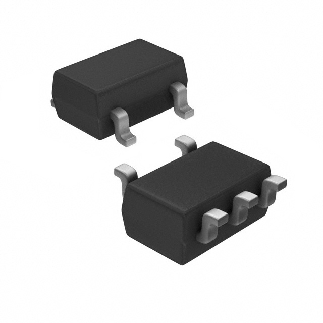
Package
The S-80949CLMC-G7KT2G is packaged in a small outline transistor (SOT) package, specifically SOT-23-5. This package provides compactness and ease of integration into various electronic devices.
Essence
The essence of S-80949CLMC-G7KT2G lies in its ability to accurately detect voltage levels within a specified range and provide a reset signal when necessary. This feature ensures proper functioning and reliability of electronic devices.
Packaging/Quantity
The S-80949CLMC-G7KT2G is typically available in reels containing 3,000 units per reel.
Specifications
- Supply Voltage Range: 1.6V to 6.0V
- Operating Temperature Range: -40°C to +85°C
- Output Type: Active low
- Quiescent Current: 1.0µA (typical)
- Accuracy: ±1.0% (±50mV) at 25°C
- Delay Time: 100ms (typical)
Detailed Pin Configuration
The S-80949CLMC-G7KT2G has a total of five pins arranged as follows:
```
| | --|1 |-- VDD --|2 |-- GND --|3 |-- RESET --|4 |-- N/C (No Connection) --|5 |-- VOUT |____| ```
Pin Description: 1. VDD: Supply voltage input 2. GND: Ground reference 3. RESET: Active low reset output 4. N/C: No connection (not internally connected) 5. VOUT: Voltage detection output
Functional Features
- Accurate voltage detection within the specified range
- Provides a reset signal when the voltage falls below the threshold
- Low quiescent current consumption, ensuring minimal power usage
- Built-in delay circuit prevents false resets due to temporary voltage fluctuations
- Compact package size allows for easy integration into various electronic devices
Advantages and Disadvantages
Advantages
- High accuracy in voltage detection
- Low power consumption
- Compact package size for easy integration
- Built-in delay circuit prevents false resets
Disadvantages
- Limited voltage detection range (1.6V to 6.0V)
- Active low reset output may not be suitable for all applications
Working Principles
The S-80949CLMC-G7KT2G operates based on a voltage divider network and a comparator. The voltage at the VOUT pin is compared with an internal reference voltage. When the voltage at VOUT falls below the threshold, the RESET pin is activated, providing a reset signal to the connected device. The built-in delay circuit ensures that temporary voltage fluctuations do not trigger false resets.
Detailed Application Field Plans
The S-80949CLMC-G7KT2G finds application in various electronic devices where accurate voltage detection and reset functionality are required. Some potential application fields include:
- Battery-powered devices: Ensures proper functioning and prevents damage due to low battery voltage.
- Microcontrollers: Provides a reset signal when the supply voltage drops below the specified level, ensuring reliable operation.
- Power management systems: Monitors voltage levels and triggers appropriate actions in case of abnormal conditions.
Detailed and Complete Alternative Models
- S-80949CLMC-G7KT2U: Similar to S-80949CLMC-G7KT2G but with an active high reset output.
- S-80949CLMC-G7KT2H: Extended temperature range version (-40°C to +125°C) of S-80949CLMC-G7KT2G.
- S-80949CLMC-G7KT2F: Lower accuracy version (±2.0%) of S-80949CLMC-G7KT2G.
These alternative models provide flexibility in choosing the most suitable product based on specific application requirements.
In conclusion, the S-80949CLMC-G7KT2G is an integrated circuit designed for accurate voltage detection and reset functions. Its compact size, low power consumption, and built-in delay circuit make it suitable for various
Enumere 10 preguntas y respuestas comunes relacionadas con la aplicación de S-80949CLMC-G7KT2G en soluciones técnicas
Sure! Here are 10 common questions and answers related to the application of S-80949CLMC-G7KT2G in technical solutions:
1. What is the S-80949CLMC-G7KT2G? - The S-80949CLMC-G7KT2G is a voltage detector IC (integrated circuit) manufactured by a specific company.
2. What is the purpose of the S-80949CLMC-G7KT2G? - The purpose of this IC is to monitor and detect voltage levels in electronic circuits.
3. What is the operating voltage range of the S-80949CLMC-G7KT2G? - The operating voltage range of this IC is typically between 1.6V and 6.0V.
4. How does the S-80949CLMC-G7KT2G work? - This IC works by comparing the input voltage with a reference voltage, and when the input voltage crosses a certain threshold, it triggers an output signal.
5. What is the output type of the S-80949CLMC-G7KT2G? - The output type of this IC is an open-drain output.
6. What is the maximum current that can be sunk by the S-80949CLMC-G7KT2G? - The maximum current that can be sunk by this IC is typically around 50mA.
7. Can the S-80949CLMC-G7KT2G be used in automotive applications? - Yes, this IC is suitable for use in automotive applications as it meets the necessary standards and requirements.
8. Is the S-80949CLMC-G7KT2G available in different package types? - Yes, this IC is available in various package types, such as SOT-23-5 and SC-82AB.
9. What is the temperature range for the S-80949CLMC-G7KT2G? - The temperature range for this IC is typically between -40°C and +85°C.
10. Can the S-80949CLMC-G7KT2G be used in battery-powered applications? - Yes, this IC can be used in battery-powered applications as it has a low quiescent current consumption, making it suitable for power-sensitive designs.
Please note that the answers provided here are general and may vary depending on the specific datasheet and manufacturer's specifications of the S-80949CLMC-G7KT2G.