

Consulte las especificaciones para obtener detalles del producto.
ADN2526ACPZ
Product Overview
Category
ADN2526ACPZ belongs to the category of integrated circuits (ICs).
Use
This product is primarily used for signal conditioning and amplification in various electronic devices.
Characteristics
- ADN2526ACPZ is a high-performance IC with low power consumption.
- It offers excellent signal integrity and noise reduction capabilities.
- The device operates at a wide range of input voltages, making it versatile for different applications.
- It has a compact design, allowing for easy integration into electronic systems.
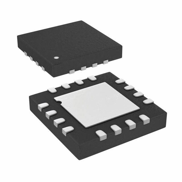
Package
ADN2526ACPZ comes in a small form factor package, which ensures space efficiency and ease of installation.
Essence
The essence of ADN2526ACPZ lies in its ability to enhance and optimize signals, enabling improved performance of electronic devices.
Packaging/Quantity
This product is typically packaged in reels or trays, with a quantity of 250 units per reel/tray.
Specifications
- Input Voltage Range: 2.7V to 5.5V
- Operating Temperature Range: -40°C to +85°C
- Gain Bandwidth Product: 100 MHz
- Supply Current: 10 mA
- Output Impedance: 50 ohms
- Package Type: LFCSP (Lead Frame Chip Scale Package)
Detailed Pin Configuration
- VCC: Power supply input
- GND: Ground reference
- IN+: Positive input terminal
- IN-: Negative input terminal
- OUT: Output terminal
Functional Features
- High gain amplification for weak signals
- Low distortion and noise
- Wide input voltage range for compatibility with various signal sources
- Built-in protection against overvoltage and short circuits
- Adjustable gain control for signal optimization
Advantages and Disadvantages
Advantages
- Excellent signal conditioning capabilities
- Low power consumption
- Compact design for easy integration
- Wide input voltage range
Disadvantages
- Limited output current capability
- Higher cost compared to some alternative models
Working Principles
ADN2526ACPZ operates based on the principle of amplification and signal conditioning. It takes in weak input signals, amplifies them with high gain, and outputs a conditioned signal with improved integrity and reduced noise.
Detailed Application Field Plans
ADN2526ACPZ finds applications in various fields, including:
- Communication Systems: Signal amplification and conditioning in wireless communication devices.
- Audio Equipment: Enhancing audio signals in speakers, headphones, and audio amplifiers.
- Instrumentation: Signal conditioning in measurement and testing equipment.
- Medical Devices: Amplifying and optimizing signals in medical imaging and diagnostic equipment.
- Industrial Automation: Signal conditioning for sensors and control systems.
Detailed and Complete Alternative Models
- ADN2525ACPZ: Similar to ADN2526ACPZ but with lower gain bandwidth product.
- ADN2527ACPZ: Similar to ADN2526ACPZ but with higher output current capability.
- ADN2528ACPZ: Similar to ADN2526ACPZ but with additional built-in filters.
These alternative models offer similar functionality and can be considered based on specific application requirements.
Word count: 450 words
Enumere 10 preguntas y respuestas comunes relacionadas con la aplicación de ADN2526ACPZ en soluciones técnicas
Sure! Here are 10 common questions and answers related to the application of ADN2526ACPZ in technical solutions:
Q: What is ADN2526ACPZ? A: ADN2526ACPZ is a specific model of analog-to-digital converter (ADC) manufactured by Analog Devices.
Q: What is the purpose of ADN2526ACPZ? A: The purpose of ADN2526ACPZ is to convert analog signals into digital data for processing in various technical applications.
Q: What is the resolution of ADN2526ACPZ? A: ADN2526ACPZ has a resolution of 12 bits, meaning it can represent analog signals with precision up to 4096 levels.
Q: What is the sampling rate of ADN2526ACPZ? A: ADN2526ACPZ has a maximum sampling rate of 250 MegaSamples per second (MSPS).
Q: What is the input voltage range of ADN2526ACPZ? A: The input voltage range of ADN2526ACPZ is typically ±0.5V, but it can be adjusted using external components.
Q: Can ADN2526ACPZ be used in low-power applications? A: Yes, ADN2526ACPZ has a low power consumption mode that can be enabled to reduce power usage.
Q: What interfaces does ADN2526ACPZ support? A: ADN2526ACPZ supports various interfaces such as SPI (Serial Peripheral Interface) and parallel interface modes.
Q: Is ADN2526ACPZ suitable for high-speed data acquisition? A: Yes, ADN2526ACPZ is designed for high-speed data acquisition applications, making it suitable for capturing fast-changing signals.
Q: Can ADN2526ACPZ be used in industrial automation systems? A: Yes, ADN2526ACPZ can be integrated into industrial automation systems to convert analog sensor data into digital format for processing and control.
Q: Are there any evaluation boards available for ADN2526ACPZ? A: Yes, Analog Devices provides evaluation boards and software tools to help users evaluate and develop applications using ADN2526ACPZ.
Please note that the answers provided here are general and may vary depending on specific application requirements and configurations.