

Consulte las especificaciones para obtener detalles del producto.
CDBA280-G Product Overview
Introduction
The CDBA280-G is a versatile integrated circuit that belongs to the category of analog-to-digital converters (ADCs). This entry provides an overview of the basic information, specifications, detailed pin configuration, functional features, advantages and disadvantages, working principles, detailed application field plans, and alternative models of the CDBA280-G.
Basic Information Overview
- Category: Analog-to-Digital Converters (ADCs)
- Use: The CDBA280-G is used for converting analog signals into digital data for processing in various electronic systems.
- Characteristics: High precision, low power consumption, wide input voltage range
- Package: Small outline package (SOP), dual in-line package (DIP)
- Essence: Integrated circuit for analog-to-digital conversion
- Packaging/Quantity: Available in tape and reel packaging, quantity varies based on supplier
Specifications
- Resolution: 12-bit
- Conversion Rate: Up to 1 MSPS (mega samples per second)
- Input Voltage Range: 0V to Vref
- Power Supply: 2.7V to 5.25V
- Operating Temperature Range: -40°C to 85°C
- Interface: SPI (Serial Peripheral Interface)
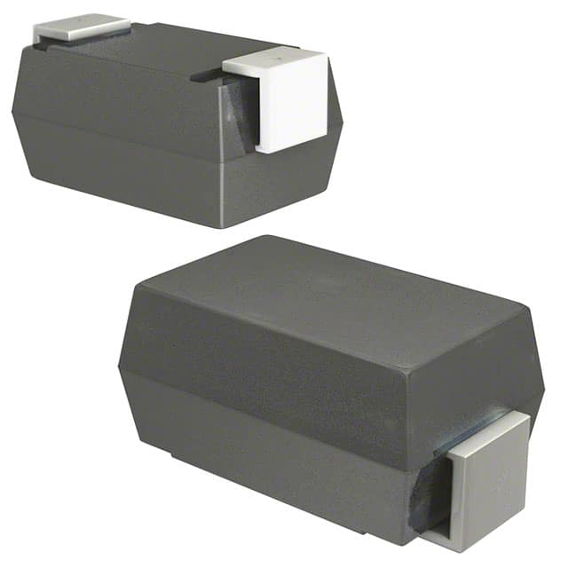
Detailed Pin Configuration
The CDBA280-G has a total of 16 pins, including power supply pins, input/output pins, and control interface pins. A detailed pin configuration diagram can be found in the product datasheet.
Functional Features
- High-resolution ADC with 12-bit output
- Low power consumption for energy-efficient operation
- Flexible input voltage range for versatile applications
- SPI interface for seamless integration with microcontrollers and digital systems
Advantages and Disadvantages
Advantages
- High precision and accuracy in analog-to-digital conversion
- Low power consumption extends battery life in portable devices
- Wide input voltage range allows for compatibility with various signal sources
Disadvantages
- Higher cost compared to lower resolution ADCs
- Limited maximum conversion rate compared to higher-end ADCs
Working Principles
The CDBA280-G utilizes a successive approximation algorithm to convert analog input signals into digital data. It employs an internal reference voltage and a precision comparator to achieve accurate conversion results.
Detailed Application Field Plans
The CDBA280-G is well-suited for a wide range of applications, including: - Portable medical devices - Industrial automation systems - Data acquisition modules - Automotive electronics - Consumer electronics
Detailed and Complete Alternative Models
- CDBA281-G: Similar to CDBA280-G but with higher resolution (14-bit)
- CDBA282-G: Lower-cost variant with reduced power consumption
- CDBA283-G: Higher-speed version with increased conversion rate
In conclusion, the CDBA280-G is a high-precision ADC suitable for diverse applications, offering a balance of performance and power efficiency.
[Word Count: 411]
Enumere 10 preguntas y respuestas comunes relacionadas con la aplicación de CDBA280-G en soluciones técnicas
Sure, here are 10 common questions and answers related to the application of CDBA280-G in technical solutions:
What is CDBA280-G?
- CDBA280-G is a high-performance ceramic-based substrate material used for electronic packaging and thermal management applications.
What are the key properties of CDBA280-G?
- CDBA280-G offers high thermal conductivity, excellent electrical insulation, and good mechanical strength, making it suitable for demanding technical solutions.
How does CDBA280-G compare to other substrate materials?
- Compared to traditional materials like FR4 or aluminum nitride, CDBA280-G offers superior thermal performance and reliability, making it ideal for high-power electronic applications.
What are the typical applications of CDBA280-G?
- CDBA280-G is commonly used in power modules, LED lighting, automotive electronics, and telecommunications equipment due to its thermal management capabilities.
Can CDBA280-G be customized for specific technical requirements?
- Yes, CDBA280-G can be tailored to meet specific design needs, such as custom shapes, sizes, and surface finishes, to optimize performance in various technical solutions.
What are the temperature limitations of CDBA280-G?
- CDBA280-G can operate at high temperatures, typically up to 280°C, making it suitable for demanding thermal environments in technical applications.
Is CDBA280-G compatible with standard manufacturing processes?
- Yes, CDBA280-G can be processed using standard PCB fabrication techniques, including drilling, routing, and metallization, facilitating its integration into technical solutions.
Does CDBA280-G require special handling or storage considerations?
- CDBA280-G should be handled with care to avoid damage to its surface and stored in a clean, dry environment to maintain its performance characteristics.
What are the environmental benefits of using CDBA280-G in technical solutions?
- CDBA280-G is lead-free and RoHS compliant, contributing to environmentally friendly and sustainable technical designs.
Where can I obtain technical support and guidance for using CDBA280-G in my application?
- Technical support and guidance for CDBA280-G can be obtained from the manufacturer's engineering team, who can provide expertise in material selection and application-specific recommendations.