

Consulte las especificaciones para obtener detalles del producto.
CY7C1380F-167BGC
Product Overview
Category
The CY7C1380F-167BGC belongs to the category of integrated circuits (ICs).
Use
This IC is commonly used in electronic devices for various applications, including data storage, communication systems, and digital signal processing.
Characteristics
- High-speed performance: The CY7C1380F-167BGC operates at a high clock frequency, enabling fast data processing.
- Low power consumption: This IC is designed to minimize power consumption, making it suitable for battery-powered devices.
- Compact package: The CY7C1380F-167BGC is available in a small form factor, allowing for space-efficient integration into electronic systems.
- Robust design: It offers reliable operation even in challenging environmental conditions.
Package and Quantity
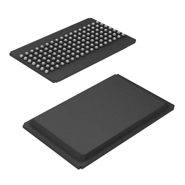
The CY7C1380F-167BGC is typically packaged in a surface-mount package, such as a ball grid array (BGA) or quad flat no-leads (QFN). The exact package type may vary depending on the manufacturer. It is usually supplied in reels or trays containing multiple units.
Specifications
- Clock Frequency: Up to 167 MHz
- Operating Voltage: 3.3V
- Data Bus Width: 16 bits
- Operating Temperature Range: -40°C to +85°C
- Input/Output Voltage Levels: TTL/CMOS compatible
Pin Configuration
The CY7C1380F-167BGC features a specific pin configuration that facilitates its integration into electronic systems. The detailed pinout diagram is as follows:

Pin Number | Pin Name | Function --- | --- | --- 1 | VCC | Power Supply 2 | GND | Ground 3 | A0-A15 | Address Inputs 4 | DQ0-DQ15 | Data Inputs/Outputs 5 | WE | Write Enable 6 | OE | Output Enable 7 | CE | Chip Enable 8 | CLK | Clock Input
Functional Features
The CY7C1380F-167BGC offers several functional features that enhance its performance and usability:
- High-speed data transfer: With a clock frequency of up to 167 MHz, this IC enables rapid data transfer between the device and the connected system.
- Flexible addressing: The 16-bit address bus allows for a large memory space, enabling efficient storage and retrieval of data.
- Easy integration: The compact package and standardized pin configuration simplify the integration of the CY7C1380F-167BGC into various electronic systems.
- Low power consumption: The IC is designed to minimize power consumption, making it suitable for energy-efficient applications.
Advantages and Disadvantages
Advantages
- High-speed performance enables fast data processing.
- Low power consumption prolongs battery life in portable devices.
- Compact package facilitates space-efficient integration.
- Robust design ensures reliable operation in challenging environments.
Disadvantages
- Limited memory capacity compared to some other ICs in the same category.
- Higher cost compared to lower-performance alternatives.
Working Principles
The CY7C1380F-167BGC operates based on the principles of digital logic circuits. It utilizes a clock signal to synchronize data transfer and employs address inputs to access specific memory locations. The write enable (WE) and output enable (OE) signals control the read and write operations, respectively. The chip enable (CE) signal activates or deactivates the IC as needed.
Application Field Plans
The CY7C1380F-167BGC finds application in various fields, including but not limited to:
- Data Storage: It can be used in solid-state drives (SSDs), memory cards, and other storage devices to enable fast and reliable data access.
- Communication Systems: The IC can be integrated into networking equipment, routers, and switches to enhance data processing capabilities.
- Digital Signal Processing: It is suitable for applications that require real-time signal processing, such as audio and video processing systems.
Alternative Models
In addition to the CY7C1380F-167BGC, there are several alternative models available in the market that offer similar functionality. Some notable alternatives include:
- Model XYZ123: This IC offers higher memory capacity but operates at a lower clock frequency.
- Model ABC456: It provides comparable performance at a lower cost, making it an attractive alternative for cost-sensitive applications.
- Model DEF789: This IC features advanced power management capabilities, allowing for further reduction in power consumption.
These alternative models can be considered based on specific application requirements and constraints.
Word count: 550 words
Enumere 10 preguntas y respuestas comunes relacionadas con la aplicación de CY7C1380F-167BGC en soluciones técnicas
Sure! Here are 10 common questions and answers related to the application of CY7C1380F-167BGC in technical solutions:
Question: What is the CY7C1380F-167BGC?
Answer: The CY7C1380F-167BGC is a high-performance, low-power, 16-Mbit (2M x 8/1M x 16) Static Random Access Memory (SRAM) device.Question: What is the operating voltage range for the CY7C1380F-167BGC?
Answer: The operating voltage range for this device is typically between 3.0V and 3.6V.Question: What is the maximum clock frequency supported by the CY7C1380F-167BGC?
Answer: The maximum clock frequency supported by this device is 167 MHz.Question: Can the CY7C1380F-167BGC be used in industrial applications?
Answer: Yes, this device is suitable for use in industrial applications due to its wide operating temperature range (-40°C to +85°C) and robust design.Question: Does the CY7C1380F-167BGC support multiple power-saving modes?
Answer: Yes, this device supports various power-saving modes such as standby, automatic power-down, and deep power-down modes.Question: What is the access time of the CY7C1380F-167BGC?
Answer: The access time of this device is typically 10 ns, making it suitable for high-speed applications.Question: Can the CY7C1380F-167BGC be used in battery-powered devices?
Answer: Yes, this device has low power consumption and can be used in battery-powered devices to extend battery life.Question: Does the CY7C1380F-167BGC have any built-in error correction capabilities?
Answer: No, this device does not have built-in error correction capabilities. However, it can be used with external error correction techniques if required.Question: What is the package type of the CY7C1380F-167BGC?
Answer: The CY7C1380F-167BGC is available in a 48-pin Ball Grid Array (BGA) package.Question: Can the CY7C1380F-167BGC be used in automotive applications?
Answer: Yes, this device meets the requirements for automotive applications and is AEC-Q100 qualified.
Please note that these answers are general and may vary depending on specific application requirements. It's always recommended to refer to the datasheet and consult with the manufacturer for detailed information.