

Consulte las especificaciones para obtener detalles del producto.
S25FL032P0XNFI001
Product Overview
- Category: Flash Memory
- Use: Data storage and retrieval in electronic devices
- Characteristics:
- Non-volatile memory
- High-speed read and write operations
- Low power consumption
- Wide temperature range (-40°C to +85°C)
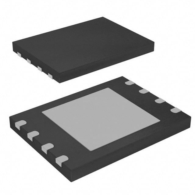
- Package: Small Outline Integrated Circuit (SOIC)
- Essence: Provides reliable and efficient data storage solution for various electronic devices
- Packaging/Quantity: Available in tape and reel packaging, with 250 units per reel
Specifications
- Memory Size: 32 Megabits (4 Megabytes)
- Interface: Serial Peripheral Interface (SPI)
- Operating Voltage: 2.7V to 3.6V
- Operating Frequency: Up to 104 MHz
- Page Size: 256 bytes
- Erase Sectors: 4 kilobytes
- Write Endurance: 100,000 cycles
- Data Retention: 20 years
Detailed Pin Configuration
The S25FL032P0XNFI001 has a total of 8 pins:
- Chip Select (/CS)
- Serial Clock (SCLK)
- Serial Data Input (SI)
- Serial Data Output (SO)
- Write Protect (/WP)
- Hold (/HOLD)
- Ground (GND)
- Power Supply (VCC)
Functional Features
- High-Speed Performance: The S25FL032P0XNFI001 offers fast read and write operations, allowing for quick data access and transfer.
- Reliability: With its non-volatile memory technology, the device ensures data retention even when power is disconnected.
- Low Power Consumption: The flash memory operates efficiently with low power requirements, making it suitable for battery-powered devices.
- Wide Temperature Range: The device can withstand extreme temperatures, enabling its use in various environments.
Advantages and Disadvantages
Advantages: - Fast read and write operations - Reliable data retention - Low power consumption - Wide temperature range suitability
Disadvantages: - Limited storage capacity compared to higher-capacity flash memory options - Higher cost per unit compared to some other memory technologies
Working Principles
The S25FL032P0XNFI001 utilizes the Serial Peripheral Interface (SPI) to communicate with the host device. It stores data in non-volatile memory cells, which retain information even when power is removed. The SPI interface allows for high-speed data transfer between the device and the host, enabling efficient storage and retrieval of data.
Detailed Application Field Plans
The S25FL032P0XNFI001 is commonly used in various electronic devices that require reliable and efficient data storage. Some application fields include:
Consumer Electronics:
- Smartphones
- Tablets
- Digital cameras
Automotive:
- Infotainment systems
- Advanced driver-assistance systems (ADAS)
Industrial:
- Internet of Things (IoT) devices
- Industrial control systems
Networking:
- Routers
- Switches
- Network attached storage (NAS)
Detailed and Complete Alternative Models
- S25FL064L0XNFI001: 64 Megabit (8 Megabyte) flash memory with similar specifications and features.
- MX25L3233FZNI-08G: 32 Megabit flash memory from Macronix with comparable characteristics and functionality.
- W25Q32JVSSIQ: 32 Megabit flash memory from Winbond offering similar performance and compatibility.
(Note: This list is not exhaustive and there may be other alternative models available in the market.)
Word count: 525 words
Enumere 10 preguntas y respuestas comunes relacionadas con la aplicación de S25FL032P0XNFI001 en soluciones técnicas
Sure! Here are 10 common questions and answers related to the application of S25FL032P0XNFI001 in technical solutions:
Q: What is the S25FL032P0XNFI001? A: The S25FL032P0XNFI001 is a serial NOR flash memory chip manufactured by Cypress Semiconductor. It offers 32 megabits (4 megabytes) of non-volatile storage.
Q: What are the typical applications of S25FL032P0XNFI001? A: The S25FL032P0XNFI001 is commonly used in various embedded systems, IoT devices, consumer electronics, automotive applications, and industrial equipment where non-volatile storage is required.
Q: What is the interface used to communicate with S25FL032P0XNFI001? A: The S25FL032P0XNFI001 uses a Serial Peripheral Interface (SPI) for communication, which is a widely supported standard interface in microcontrollers and other devices.
Q: What is the maximum data transfer rate supported by S25FL032P0XNFI001? A: The S25FL032P0XNFI001 supports a maximum SPI clock frequency of 104 MHz, allowing for fast data transfers.
Q: Can S25FL032P0XNFI001 be easily integrated into existing designs? A: Yes, the S25FL032P0XNFI001 is designed to be compatible with industry-standard footprints and pinouts, making it relatively easy to integrate into existing designs.
Q: Does S25FL032P0XNFI001 support hardware and software protection features? A: Yes, the S25FL032P0XNFI001 provides hardware and software protection features like write protection, block protection, and sector protection to prevent accidental or unauthorized modifications.
Q: What is the typical power supply voltage range for S25FL032P0XNFI001? A: The S25FL032P0XNFI001 operates with a typical power supply voltage range of 2.7V to 3.6V.
Q: Can S25FL032P0XNFI001 operate in extreme temperature conditions? A: Yes, the S25FL032P0XNFI001 is designed to operate reliably in a wide temperature range, typically from -40°C to +85°C.
Q: Does S25FL032P0XNFI001 support over-the-air (OTA) firmware updates? A: Yes, the S25FL032P0XNFI001 can be used to store firmware or software updates, allowing for OTA updates in devices that support it.
Q: Are there any development tools or software libraries available for S25FL032P0XNFI001? A: Cypress provides various development tools, software libraries, and documentation to assist developers in integrating and programming the S25FL032P0XNFI001 in their applications.
Please note that the answers provided here are general and may vary depending on specific implementation details and requirements.