

Consulte las especificaciones para obtener detalles del producto.
S25FL208K0RMFI040
Basic Information Overview
- Category: Flash Memory
- Use: Data storage and retrieval in electronic devices
- Characteristics:
- Non-volatile memory
- High-speed read and write operations
- Low power consumption
- Wide temperature range (-40°C to +85°C)
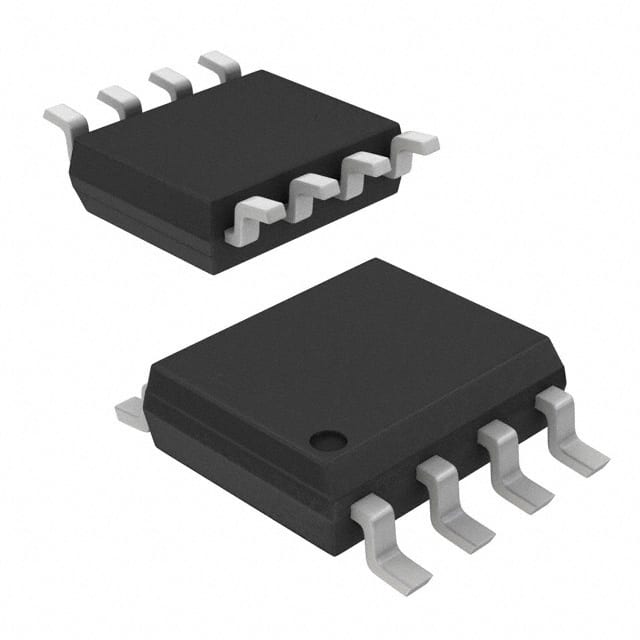
- Package: 8-pin SOIC (Small Outline Integrated Circuit)
- Essence: Reliable and efficient flash memory solution
- Packaging/Quantity: Available in reels of 2500 units
Specifications
- Memory Capacity: 8 Megabits (1 Megabyte)
- Interface: Serial Peripheral Interface (SPI)
- Voltage Range: 2.7V to 3.6V
- Operating Frequency: Up to 104 MHz
- Erase/Program Operations:
- Sector Erase Time: 100 ms (typical)
- Page Program Time: 0.75 ms (typical)
- Data Retention: 20 years (minimum)
Detailed Pin Configuration
- Chip Select (/CS)
- Serial Clock (SCLK)
- Serial Data Input (SI)
- Serial Data Output (SO)
- Write Protect (/WP)
- Hold (/HOLD)
- Ground (GND)
- Power Supply (VCC)
Functional Features
- Uniform 4KB sectors for easy data management
- Efficient program and erase operations
- Software and hardware protection mechanisms
- Flexible sector protection settings
- Fast read access time
- Automatic sleep mode for power saving
Advantages
- High-speed data transfer
- Low power consumption
- Wide operating temperature range
- Reliable and durable
- Easy integration into various electronic devices
Disadvantages
- Limited storage capacity compared to higher-end flash memory options
- Relatively higher cost per megabyte compared to larger capacity flash memory chips
Working Principles
The S25FL208K0RMFI040 operates based on the Serial Peripheral Interface (SPI) protocol. It uses a combination of electrical signals and commands to perform read, write, and erase operations. The data is stored in non-volatile memory cells that retain information even when power is removed.
Detailed Application Field Plans
- Consumer Electronics: Smartphones, tablets, digital cameras
- Automotive: Infotainment systems, instrument clusters
- Industrial: Embedded systems, control units
- Networking: Routers, switches, modems
- Medical: Patient monitoring devices, diagnostic equipment
Detailed and Complete Alternative Models
- S25FL116K0RMFI010 - 16 Megabits (2 Megabytes)
- S25FL032K0RMFI040 - 32 Megabits (4 Megabytes)
- S25FL064K0RMFI100 - 64 Megabits (8 Megabytes)
- S25FL128K0RMFI010 - 128 Megabits (16 Megabytes)
- S25FL256SAGMFI011 - 256 Megabits (32 Megabytes)
Note: These are just a few examples; there are several other alternative models available in the market.
This entry provides an overview of the S25FL208K0RMFI040 flash memory chip, including its basic information, specifications, pin configuration, functional features, advantages, disadvantages, working principles, application field plans, and alternative models. With its reliable performance and wide range of applications, the S25FL208K0RMFI040 is a valuable flash memory solution for various electronic devices.
Enumere 10 preguntas y respuestas comunes relacionadas con la aplicación de S25FL208K0RMFI040 en soluciones técnicas
Sure! Here are 10 common questions and answers related to the application of S25FL208K0RMFI040 in technical solutions:
Q: What is the S25FL208K0RMFI040? A: The S25FL208K0RMFI040 is a serial NOR flash memory chip manufactured by Cypress Semiconductor.
Q: What is the storage capacity of the S25FL208K0RMFI040? A: The S25FL208K0RMFI040 has a storage capacity of 8 megabits (1 megabyte).
Q: What is the interface used to communicate with the S25FL208K0RMFI040? A: The S25FL208K0RMFI040 uses a Serial Peripheral Interface (SPI) for communication.
Q: What voltage levels does the S25FL208K0RMFI040 support? A: The S25FL208K0RMFI040 supports both 3.3V and 1.8V voltage levels.
Q: Can the S25FL208K0RMFI040 be used for code execution? A: Yes, the S25FL208K0RMFI040 can be used for executing code directly from the flash memory.
Q: Is the S25FL208K0RMFI040 suitable for high-speed data transfer? A: Yes, the S25FL208K0RMFI040 supports high-speed read and write operations, making it suitable for data-intensive applications.
Q: Does the S25FL208K0RMFI040 have built-in security features? A: Yes, the S25FL208K0RMFI040 provides hardware-based security features like sector protection and password protection.
Q: Can the S25FL208K0RMFI040 operate in extreme temperature conditions? A: Yes, the S25FL208K0RMFI040 has a wide operating temperature range of -40°C to +85°C.
Q: Can multiple S25FL208K0RMFI040 chips be cascaded together? A: Yes, multiple S25FL208K0RMFI040 chips can be cascaded together using the SPI interface for increased storage capacity.
Q: Is the S25FL208K0RMFI040 compatible with different microcontrollers? A: Yes, the S25FL208K0RMFI040 is compatible with various microcontrollers that support SPI communication.
Please note that these answers are general and may vary depending on specific implementation details and requirements.