

Consulte las especificaciones para obtener detalles del producto.
Encyclopedia Entry: 74AUP1G86FS3-7
Product Overview
Category
The 74AUP1G86FS3-7 belongs to the category of integrated circuits (ICs).
Use
This IC is commonly used in electronic devices for signal processing and logic operations.
Characteristics
- Low power consumption
- High-speed operation
- Wide operating voltage range
- Small package size
Package
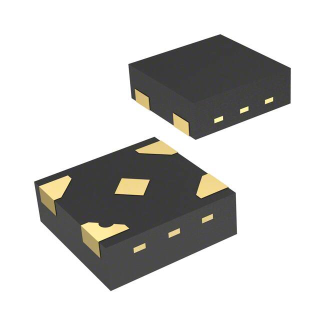
The 74AUP1G86FS3-7 is available in a small form factor package, such as SOT-353 or DFN1006-3.
Essence
This IC is designed to provide efficient and reliable logic gate functionality in various electronic applications.
Packaging/Quantity
The 74AUP1G86FS3-7 is typically packaged in reels or tubes, with quantities varying depending on the manufacturer's specifications.
Specifications
- Supply Voltage Range: 0.8V to 3.6V
- Logic Family: AUP
- Number of Gates: 1
- Input/Output Compatibility: CMOS/TTL
- Operating Temperature Range: -40°C to +85°C
Detailed Pin Configuration
The 74AUP1G86FS3-7 has the following pin configuration:
```
| | --| A | --| B Y | --| GND | --| VCC | |___________| ```
Functional Features
- XOR gate functionality: The 74AUP1G86FS3-7 performs exclusive OR (XOR) logic operations on its input signals.
- High-speed operation: This IC can process logic operations at a fast rate, making it suitable for time-critical applications.
- Low power consumption: The 74AUP1G86FS3-7 is designed to minimize power consumption, making it ideal for battery-powered devices.
Advantages and Disadvantages
Advantages
- Small package size allows for space-efficient designs.
- Wide operating voltage range enables compatibility with various power supply configurations.
- Low power consumption prolongs battery life in portable devices.
Disadvantages
- Limited number of gates (1 gate) may restrict its use in complex logic circuits.
- Availability and pricing may vary depending on the manufacturer and market demand.
Working Principles
The 74AUP1G86FS3-7 operates based on the principles of CMOS logic. It utilizes MOSFET transistors to implement XOR gate functionality. When input signals are applied, the IC processes them to produce the corresponding output signal according to the XOR truth table.
Detailed Application Field Plans
The 74AUP1G86FS3-7 finds applications in various electronic systems, including but not limited to: - Mobile devices - Consumer electronics - Communication equipment - Industrial automation - Automotive electronics
Detailed and Complete Alternative Models
- 74AUP1G86GM
- SN74AUP1G86DCKR
- MC74AUP1G86DTT1G
These alternative models offer similar functionality and can be used as substitutes for the 74AUP1G86FS3-7 in different applications.
In conclusion, the 74AUP1G86FS3-7 is a versatile integrated circuit that provides XOR gate functionality with low power consumption and high-speed operation. Its small package size and wide operating voltage range make it suitable for various electronic applications. However, its limited number of gates and availability may pose some limitations.
Enumere 10 preguntas y respuestas comunes relacionadas con la aplicación de 74AUP1G86FS3-7 en soluciones técnicas
Sure! Here are 10 common questions and answers related to the application of 74AUP1G86FS3-7 in technical solutions:
Q1: What is the 74AUP1G86FS3-7? A1: The 74AUP1G86FS3-7 is a single 2-input XOR gate IC (integrated circuit) that operates at a voltage range of 0.8V to 3.6V.
Q2: What is the purpose of the 74AUP1G86FS3-7? A2: The purpose of this IC is to perform XOR (exclusive OR) logic operations, which are commonly used in digital circuits for various applications such as data encryption, error detection, and signal processing.
Q3: What is the maximum operating frequency of the 74AUP1G86FS3-7? A3: The maximum operating frequency of this IC is typically around 500 MHz, making it suitable for high-speed digital applications.
Q4: What is the power supply voltage range for the 74AUP1G86FS3-7? A4: The power supply voltage range for this IC is from 0.8V to 3.6V, allowing it to be used in low-power and battery-operated devices.
Q5: Can the 74AUP1G86FS3-7 be used with other logic families? A5: Yes, this IC is compatible with a wide range of logic families, including TTL (Transistor-Transistor Logic), CMOS (Complementary Metal-Oxide-Semiconductor), and LVCMOS (Low-Voltage CMOS).
Q6: What is the input/output voltage level compatibility of the 74AUP1G86FS3-7? A6: The input voltage levels are compatible with both CMOS and TTL logic levels, while the output voltage levels are compatible with CMOS logic levels.
Q7: What is the package type of the 74AUP1G86FS3-7? A7: This IC is available in a small SOT353 package, which is suitable for space-constrained applications.
Q8: Can the 74AUP1G86FS3-7 be used in automotive applications? A8: Yes, this IC is AEC-Q100 qualified, making it suitable for use in automotive electronics applications that require high reliability and performance.
Q9: Does the 74AUP1G86FS3-7 have any built-in protection features? A9: Yes, this IC has built-in ESD (Electrostatic Discharge) protection, ensuring its robustness against electrostatic discharge events during handling and operation.
Q10: Where can I find more information about the 74AUP1G86FS3-7? A10: You can refer to the datasheet provided by the manufacturer or visit their official website for detailed information on the electrical characteristics, pin configuration, and application notes of the 74AUP1G86FS3-7.