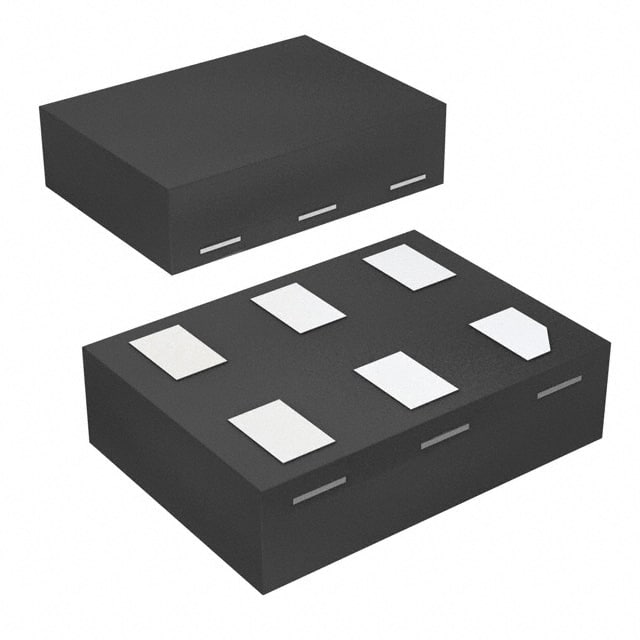
Consulte las especificaciones para obtener detalles del producto.

Encyclopedia Entry: 74AUP2G14FZ4-7
Product Overview
Category
The 74AUP2G14FZ4-7 belongs to the category of integrated circuits (ICs), specifically a dual inverter gate.
Use
This IC is commonly used in digital logic circuits for signal inversion and amplification purposes.
Characteristics
- Low power consumption
- High-speed operation
- Wide operating voltage range
- Small package size
- RoHS compliant
Package
The 74AUP2G14FZ4-7 is available in a small form factor package, such as a flip-chip package or a leadless package. The specific package type may vary depending on the manufacturer.
Essence
The essence of the 74AUP2G14FZ4-7 lies in its ability to provide reliable and efficient signal inversion and amplification within digital logic circuits.
Packaging/Quantity
Typically, the 74AUP2G14FZ4-7 is sold in reels or tubes, with quantities varying based on the manufacturer's packaging standards. Common quantities include 250, 500, or 1000 units per reel/tube.
Specifications
- Supply Voltage Range: 0.8V to 3.6V
- Input Voltage Range: 0V to VCC
- Output Voltage Range: 0V to VCC
- Operating Temperature Range: -40°C to +85°C
- Maximum Propagation Delay: 5 ns
- Maximum Quiescent Current: 1 μA
Detailed Pin Configuration
The 74AUP2G14FZ4-7 has a total of 6 pins, labeled as follows:
- IN1: Input 1
- OUT1: Output 1
- GND: Ground
- IN2: Input 2
- OUT2: Output 2
- VCC: Power Supply
Functional Features
- Dual inverter gate functionality
- High-speed signal inversion and amplification
- Low power consumption
- Wide operating voltage range for compatibility with various systems
- Compact size for space-constrained applications
Advantages and Disadvantages
Advantages
- Low power consumption makes it suitable for battery-powered devices
- High-speed operation enables efficient signal processing
- Wide operating voltage range allows for compatibility with different voltage levels
- Small package size saves board space in compact designs
Disadvantages
- Limited number of inputs and outputs compared to more complex ICs
- May not be suitable for applications requiring advanced logic functions
Working Principles
The 74AUP2G14FZ4-7 operates based on the principles of complementary metal-oxide-semiconductor (CMOS) technology. It utilizes a combination of p-type and n-type MOSFETs to achieve signal inversion and amplification.
Detailed Application Field Plans
The 74AUP2G14FZ4-7 finds application in various digital logic circuits, including but not limited to: - Microcontrollers - Data communication systems - Signal processing units - Consumer electronics - Industrial automation
Detailed and Complete Alternative Models
Some alternative models that offer similar functionality to the 74AUP2G14FZ4-7 include: - SN74LVC2G04 from Texas Instruments - MC74VHC1G14 from ON Semiconductor - 74HC04 from NXP Semiconductors
These alternatives may have slight variations in specifications and pin configurations, so it is important to consult the respective datasheets for detailed information.
In conclusion, the 74AUP2G14FZ4-7 is a dual inverter gate IC that offers high-speed signal inversion and amplification with low power consumption. Its compact size and wide operating voltage range make it suitable for various digital logic circuit applications. However, it is important to consider alternative models based on specific requirements and compatibility.
Enumere 10 preguntas y respuestas comunes relacionadas con la aplicación de 74AUP2G14FZ4-7 en soluciones técnicas
Sure! Here are 10 common questions and answers related to the application of 74AUP2G14FZ4-7 in technical solutions:
Q: What is the 74AUP2G14FZ4-7? A: The 74AUP2G14FZ4-7 is a dual Schmitt-trigger inverter IC, commonly used in digital logic circuits.
Q: What is the operating voltage range of the 74AUP2G14FZ4-7? A: The operating voltage range of the 74AUP2G14FZ4-7 is typically between 0.8V and 3.6V.
Q: Can the 74AUP2G14FZ4-7 be used in battery-powered applications? A: Yes, the low operating voltage range makes it suitable for battery-powered applications.
Q: What is the maximum output current of the 74AUP2G14FZ4-7? A: The maximum output current of the 74AUP2G14FZ4-7 is typically around 32mA.
Q: Is the 74AUP2G14FZ4-7 compatible with both CMOS and TTL logic levels? A: Yes, the 74AUP2G14FZ4-7 is compatible with both CMOS and TTL logic levels.
Q: Can the 74AUP2G14FZ4-7 be used as a level shifter? A: Yes, the 74AUP2G14FZ4-7 can be used as a level shifter to convert signals between different voltage levels.
Q: Does the 74AUP2G14FZ4-7 have built-in protection against overvoltage? A: No, the 74AUP2G14FZ4-7 does not have built-in overvoltage protection. External measures may be required.
Q: What is the maximum operating frequency of the 74AUP2G14FZ4-7? A: The maximum operating frequency of the 74AUP2G14FZ4-7 is typically around 200MHz.
Q: Can the 74AUP2G14FZ4-7 be used in high-speed data transmission applications? A: Yes, the 74AUP2G14FZ4-7 can be used in high-speed data transmission applications due to its fast switching speed.
Q: Is the 74AUP2G14FZ4-7 available in different package options? A: Yes, the 74AUP2G14FZ4-7 is available in various package options, such as SOT353 and XSON6.

