

Consulte las especificaciones para obtener detalles del producto.
74LVC1G32SE-7
Product Overview
Category
The 74LVC1G32SE-7 belongs to the category of integrated circuits (ICs).
Use
This IC is commonly used in digital logic applications, specifically for performing logical OR operations.
Characteristics
- Low-voltage CMOS technology
- High-speed operation
- Wide operating voltage range
- Low power consumption
- Schmitt-trigger input for noise immunity
- Small package size
Package
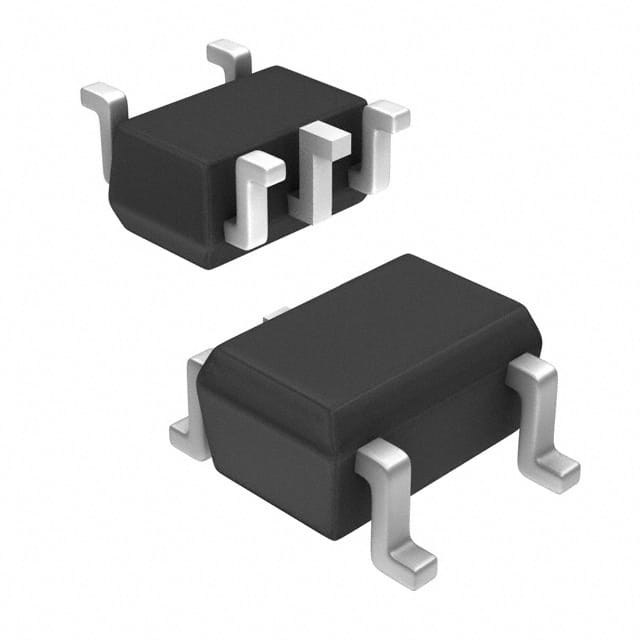
The 74LVC1G32SE-7 is available in a small SOT-353 package.
Essence
The essence of the 74LVC1G32SE-7 lies in its ability to perform logical OR operations efficiently and reliably in various digital logic circuits.
Packaging/Quantity
The IC is typically packaged in reels or tubes, with a quantity of 3000 units per reel/tube.
Specifications
- Supply Voltage Range: 1.65V to 5.5V
- Input Voltage Range: 0V to VCC
- Output Voltage Range: 0V to VCC
- Operating Temperature Range: -40°C to +125°C
- Propagation Delay: 4.3 ns (typical)
- Maximum Quiescent Current: 10 μA
Detailed Pin Configuration
The 74LVC1G32SE-7 has a total of five pins:
- GND (Ground): Connected to the ground reference.
- A (Input): First input pin for logical OR operation.
- B (Input): Second input pin for logical OR operation.
- Y (Output): Output pin providing the result of the logical OR operation.
- VCC (Power): Connected to the positive supply voltage.
Functional Features
The key functional features of the 74LVC1G32SE-7 include:
- Logical OR operation: The IC performs a logical OR operation on the input signals A and B, providing the result at the output pin Y.
- Schmitt-trigger input: The Schmitt-trigger input ensures noise immunity by providing hysteresis to the input signals.
Advantages and Disadvantages
Advantages
- Low power consumption makes it suitable for battery-powered devices.
- Wide operating voltage range allows compatibility with various systems.
- Small package size saves board space in compact designs.
- High-speed operation enables efficient data processing.
Disadvantages
- Limited number of inputs (only two) restricts its application in complex logic circuits.
- Lack of built-in protection features may require additional circuitry for robustness.
Working Principles
The 74LVC1G32SE-7 operates based on CMOS technology. It utilizes MOSFET transistors to perform logical OR operations. When both input signals A and B are low, the output Y remains low. If either or both inputs are high, the output Y becomes high, indicating the logical OR result.
Detailed Application Field Plans
The 74LVC1G32SE-7 finds applications in various digital systems, including but not limited to: - Microcontrollers - Data communication devices - Consumer electronics - Automotive electronics - Industrial control systems
Detailed and Complete Alternative Models
Some alternative models that can be used as substitutes for the 74LVC1G32SE-7 include: - SN74LVC1G32DBVR - MC74VHC1G32DTT1G - TC7SZ32FU
These alternatives offer similar functionality and characteristics, allowing flexibility in design choices.
In conclusion, the 74LVC1G32SE-7 is a versatile integrated circuit used for logical OR operations in digital logic circuits. Its low power consumption, wide operating voltage range, and small package size make it suitable for various applications. However, its limited number of inputs and lack of built-in protection features should be considered when selecting this IC for specific designs.
Enumere 10 preguntas y respuestas comunes relacionadas con la aplicación de 74LVC1G32SE-7 en soluciones técnicas
Sure! Here are 10 common questions and answers related to the application of 74LVC1G32SE-7 in technical solutions:
Q1: What is the 74LVC1G32SE-7? A1: The 74LVC1G32SE-7 is a single 2-input OR gate IC (integrated circuit) that operates at a voltage level of 3.3V.
Q2: What is the purpose of an OR gate? A2: An OR gate is a logic gate that performs logical OR operation on its inputs. It outputs a high signal if any of its inputs are high.
Q3: What are the typical applications of the 74LVC1G32SE-7? A3: The 74LVC1G32SE-7 can be used in various applications such as signal conditioning, data transmission, and general-purpose logic functions.
Q4: What is the maximum operating frequency of the 74LVC1G32SE-7? A4: The maximum operating frequency of the 74LVC1G32SE-7 is typically around 200 MHz.
Q5: What is the input voltage range for the 74LVC1G32SE-7? A5: The input voltage range for the 74LVC1G32SE-7 is from ground (0V) to VCC (3.3V).
Q6: Can the 74LVC1G32SE-7 operate at different voltage levels? A6: No, the 74LVC1G32SE-7 is specifically designed to operate at a voltage level of 3.3V.
Q7: How many inputs does the 74LVC1G32SE-7 have? A7: The 74LVC1G32SE-7 has two inputs.
Q8: What is the output voltage level of the 74LVC1G32SE-7? A8: The output voltage level of the 74LVC1G32SE-7 is the same as the supply voltage, which is typically 3.3V.
Q9: Can the 74LVC1G32SE-7 be used in battery-powered applications? A9: Yes, the 74LVC1G32SE-7 can be used in battery-powered applications as it operates at a low voltage level of 3.3V.
Q10: Is the 74LVC1G32SE-7 available in different package options? A10: Yes, the 74LVC1G32SE-7 is available in various package options such as SOT23 and SC-70.
Please note that these answers are general and may vary depending on the specific datasheet and manufacturer's specifications for the 74LVC1G32SE-7.