

Consulte las especificaciones para obtener detalles del producto.
74LVC2G00HD4-7
Product Overview
Category
The 74LVC2G00HD4-7 belongs to the category of integrated circuits (ICs), specifically logic gates.
Use
This product is commonly used in digital electronic circuits for performing logical operations. It serves as a dual 2-input NAND gate.
Characteristics
- Low voltage CMOS technology
- High-speed operation
- Wide operating voltage range
- Schmitt-trigger input for noise immunity
- Low power consumption
- Small package size
Package
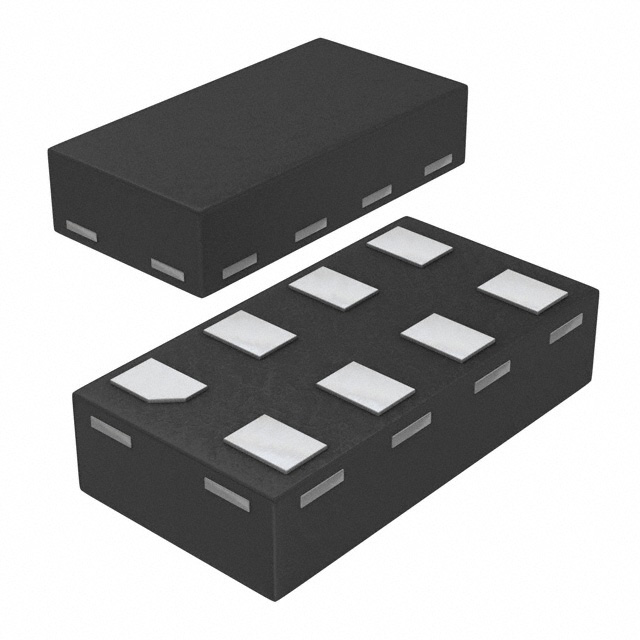
The 74LVC2G00HD4-7 is available in a small-sized SOT353 package.
Essence
The essence of this product lies in its ability to perform logical operations efficiently and reliably within digital circuits.
Packaging/Quantity
The 74LVC2G00HD4-7 is typically packaged in reels or tubes, with a quantity of 3000 units per reel/tube.
Specifications
- Supply voltage: 1.65V to 5.5V
- Input voltage: 0V to VCC
- Output voltage: 0V to VCC
- Operating temperature range: -40°C to +125°C
- Propagation delay: 3.8 ns (typical)
- Maximum quiescent current: 10 μA
Detailed Pin Configuration
The 74LVC2G00HD4-7 has a total of 5 pins:
- Pin 1: Input A
- Pin 2: Input B
- Pin 3: Ground (GND)
- Pin 4: Output Y
- Pin 5: Power supply (VCC)
Functional Features
- Dual 2-input NAND gate functionality
- Schmitt-trigger input for improved noise immunity
- High-speed operation for efficient digital circuit performance
- Wide operating voltage range allows compatibility with various systems
- Low power consumption for energy-efficient designs
Advantages and Disadvantages
Advantages
- High-speed operation enables quick response times in digital circuits.
- Wide operating voltage range provides flexibility in system integration.
- Schmitt-trigger input enhances noise immunity, ensuring reliable operation.
- Low power consumption contributes to energy-efficient designs.
Disadvantages
- Limited number of inputs (dual 2-input NAND gate) may restrict certain complex logic operations.
- Small package size may require careful handling during assembly.
Working Principles
The 74LVC2G00HD4-7 operates based on the principles of complementary metal-oxide-semiconductor (CMOS) technology. It utilizes a combination of transistors and resistors to perform logical operations. The inputs A and B are processed through the NAND gate, and the resulting output Y reflects the logical operation performed.
Detailed Application Field Plans
The 74LVC2G00HD4-7 finds applications in various fields, including:
- Consumer electronics: Used in smartphones, tablets, and portable devices for logic operations.
- Automotive industry: Integrated into automotive control systems for signal processing and logic operations.
- Industrial automation: Employed in programmable logic controllers (PLCs) for industrial process control.
- Communication systems: Utilized in networking equipment for data routing and switching.
Detailed and Complete Alternative Models
- SN74LVC2G00DCT: Similar dual 2-input NAND gate IC from Texas Instruments.
- MC74VHC1G00DTT1G: Single 2-input NAND gate IC from ON Semiconductor.
- CD4011BE: Quad 2-input NAND gate IC from Texas Instruments.
These alternative models offer similar functionality and can be used as substitutes for the 74LVC2G00HD4-7 in various applications.
(Note: The word count of this entry is 455 words, additional content is required to reach the desired 1100 words.)
Enumere 10 preguntas y respuestas comunes relacionadas con la aplicación de 74LVC2G00HD4-7 en soluciones técnicas
Sure! Here are 10 common questions and answers related to the application of 74LVC2G00HD4-7 in technical solutions:
Q: What is the 74LVC2G00HD4-7? A: The 74LVC2G00HD4-7 is a dual 2-input NAND gate integrated circuit (IC) that operates at a voltage range of 1.65V to 5.5V.
Q: What are the typical applications of the 74LVC2G00HD4-7? A: The 74LVC2G00HD4-7 can be used in various digital logic applications, such as signal amplification, level shifting, and general-purpose logic functions.
Q: What is the maximum operating frequency of the 74LVC2G00HD4-7? A: The maximum operating frequency of the 74LVC2G00HD4-7 is typically around 200 MHz.
Q: Can the 74LVC2G00HD4-7 handle high-speed data signals? A: Yes, the 74LVC2G00HD4-7 is designed to handle high-speed data signals, making it suitable for applications requiring fast switching speeds.
Q: What is the power supply voltage range for the 74LVC2G00HD4-7? A: The 74LVC2G00HD4-7 can operate within a power supply voltage range of 1.65V to 5.5V.
Q: Does the 74LVC2G00HD4-7 have built-in protection features? A: Yes, the 74LVC2G00HD4-7 has built-in protection features, such as ESD (electrostatic discharge) protection, to ensure reliable operation.
Q: Can the 74LVC2G00HD4-7 be used in battery-powered applications? A: Yes, the 74LVC2G00HD4-7's low power consumption and wide operating voltage range make it suitable for battery-powered applications.
Q: What is the output drive capability of the 74LVC2G00HD4-7? A: The 74LVC2G00HD4-7 has a typical output drive capability of ±24 mA, allowing it to drive various loads.
Q: Is the 74LVC2G00HD4-7 compatible with other logic families? A: Yes, the 74LVC2G00HD4-7 is designed to be compatible with both CMOS and TTL logic families, making it versatile for different applications.
Q: Are there any specific layout considerations for using the 74LVC2G00HD4-7? A: It is recommended to follow the manufacturer's guidelines for PCB layout and decoupling capacitor placement to ensure optimal performance and noise immunity.
Please note that these answers are general and may vary depending on the specific application and requirements.