

Consulte las especificaciones para obtener detalles del producto.
PI49FCT3805CQEX
Overview
Category
The PI49FCT3805CQEX belongs to the category of integrated circuits (ICs).
Use
It is commonly used in electronic devices for signal transmission and processing.
Characteristics
- High-speed operation
- Low power consumption
- Wide operating voltage range
- Small package size
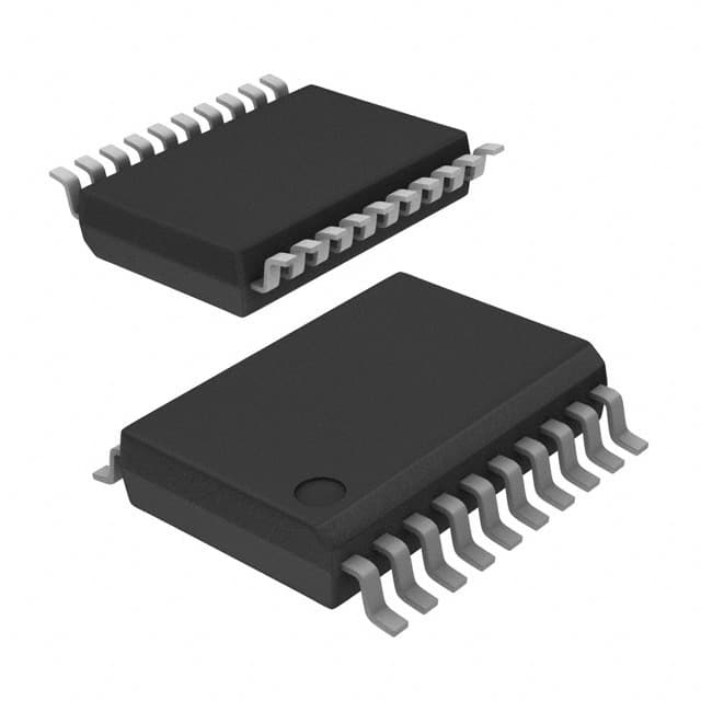
Package
The PI49FCT3805CQEX is available in a compact surface mount package.
Essence
This IC is designed to provide reliable and efficient signal transmission within electronic systems.
Packaging/Quantity
The PI49FCT3805CQEX is typically packaged in reels or trays, with a quantity of 2500 units per reel/tray.
Specifications and Parameters
- Operating Voltage: 2.3V to 3.6V
- Input Voltage Range: 0V to VCC
- Output Voltage Range: 0V to VCC
- Operating Temperature Range: -40°C to +85°C
- Input Capacitance: 4pF (typical)
- Output Capacitance: 6pF (typical)
Pin Configuration
The PI49FCT3805CQEX has a total of 8 pins, which are labeled as follows:
- VCC
- GND
- A
- B
- Y
- GND
- C
- D
Functional Characteristics
The PI49FCT3805CQEX is a quad bus buffer that provides non-inverting level shifting and signal buffering capabilities. It operates at high speeds and can handle both TTL and CMOS logic levels.
Advantages and Disadvantages
Advantages
- High-speed operation allows for efficient signal transmission
- Low power consumption helps conserve energy
- Wide operating voltage range provides flexibility in various applications
- Small package size saves board space
Disadvantages
- Limited number of input/output channels
- May require additional components for certain applications
Applicable Range of Products
The PI49FCT3805CQEX is suitable for use in a wide range of electronic devices, including but not limited to: - Computers and laptops - Telecommunications equipment - Consumer electronics - Industrial control systems
Working Principles
The PI49FCT3805CQEX works by receiving input signals from the A, B, C, and D pins and providing buffered output signals at the Y pin. It ensures proper signal levels and impedance matching between different parts of an electronic system.
Detailed Application Field Plans
The PI49FCT3805CQEX can be used in various applications, such as: 1. Data communication interfaces 2. Memory address decoding 3. Clock distribution networks 4. Bus driving and buffering 5. Signal level shifting
Detailed Alternative Models
Some alternative models to the PI49FCT3805CQEX include: - SN74LVC8T245 - MC74LVX245 - 74HC245 - CD74HCT245 - NC7WZ245
5 Common Technical Questions and Answers
Q: What is the maximum operating voltage for the PI49FCT3805CQEX? A: The maximum operating voltage is 3.6V.
Q: Can the PI49FCT3805CQEX handle both TTL and CMOS logic levels? A: Yes, it is designed to work with both TTL and CMOS logic levels.
Q: What is the typical input capacitance of the PI49FCT3805CQEX? A: The typical input capacitance is 4pF.
Q: Does the PI49FCT3805CQEX require external components for operation? A: In most cases, it can be used standalone. However, additional components may be required depending on the specific application.
Q: What is the temperature range in which the PI49FCT3805CQEX can operate? A: It can operate within a temperature range of -40°C to +85°C.
This concludes the encyclopedia entry for the PI49FCT3805CQEX.