

Consulte las especificaciones para obtener detalles del producto.
PI49FCT3807CQE
Overview
Category
PI49FCT3807CQE belongs to the category of integrated circuits (ICs).
Use
It is commonly used as a buffer/driver for various digital applications.
Characteristics
- High-speed operation
- Low power consumption
- Wide operating voltage range
- Small package size
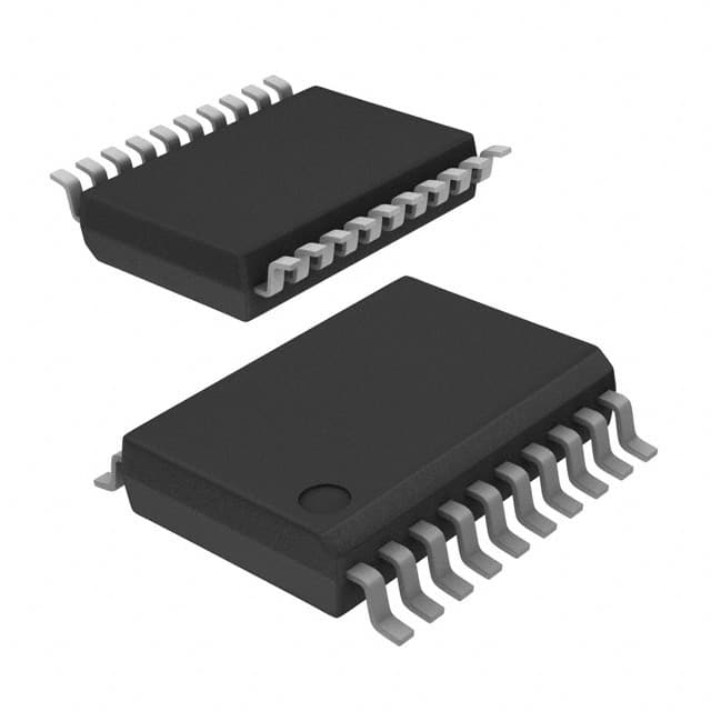
Package
PI49FCT3807CQE is available in a compact surface mount package.
Essence
The essence of PI49FCT3807CQE lies in its ability to provide efficient buffering and driving capabilities for digital signals.
Packaging/Quantity
This product is typically packaged in reels or trays, with a quantity of 2500 units per reel/tray.
Specifications and Parameters
- Supply Voltage: 2.3V to 5.5V
- Input Voltage: 0V to VCC
- Output Voltage: 0V to VCC
- Operating Temperature Range: -40°C to +85°C
- Output Current: ±24mA
Pin Configuration
The detailed pin configuration of PI49FCT3807CQE is as follows:
| Pin Number | Pin Name | Description | |------------|----------|-------------| | 1 | GND | Ground | | 2 | A | Input A | | 3 | B | Input B | | 4 | Y | Output Y | | 5 | OE | Output Enable | | 6 | VCC | Power Supply |
Functional Characteristics
- Buffering and driving digital signals
- High-speed signal propagation
- Low output impedance
- Output enable/disable control
Advantages and Disadvantages
Advantages
- High-speed operation allows for efficient signal transmission
- Low power consumption helps conserve energy
- Wide operating voltage range provides flexibility in various applications
- Small package size saves board space
Disadvantages
- Limited output current may not be suitable for high-power applications
- Lack of built-in protection features
Applicable Range of Products
PI49FCT3807CQE is widely applicable in digital systems, including but not limited to: - Microcontrollers - Digital signal processors - Communication devices - Computer peripherals
Working Principles
PI49FCT3807CQE works by receiving digital input signals and buffering/driving them to the output pin. The output enable pin allows for control over the output state.
Detailed Application Field Plans
PI49FCT3807CQE can be used in various applications, such as: 1. Interface level shifting 2. Clock distribution 3. Bus driving 4. Signal buffering 5. Logic level conversion
Detailed Alternative Models
Some alternative models to PI49FCT3807CQE include: - SN74LVC1G07DBVR - MC74VHC1GT07DTT1G - 74LVC1G07GW
5 Common Technical Questions and Answers
Q: What is the maximum operating voltage for PI49FCT3807CQE? A: The maximum operating voltage is 5.5V.
Q: Can PI49FCT3807CQE drive high-current loads? A: No, it has a limited output current of ±24mA.
Q: What is the typical power consumption of PI49FCT3807CQE? A: The typical power consumption is low due to its efficient design.
Q: Can PI49FCT3807CQE operate in extreme temperature conditions? A: Yes, it has an operating temperature range of -40°C to +85°C.
Q: Is PI49FCT3807CQE suitable for level shifting applications? A: Yes, it can be used for interface level shifting due to its wide operating voltage range.
This concludes the encyclopedia entry for PI49FCT3807CQE.