

Consulte las especificaciones para obtener detalles del producto.
PI6CG18201ZDIEX
Overview
- Category: Integrated Circuit
- Use: Clock Generator and Buffer
- Characteristics: Low jitter, high frequency, low power consumption
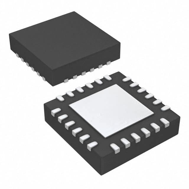
- Package: 48-pin QFN
- Essence: Clock generation and buffering for electronic devices
- Packaging/Quantity: Tape and Reel, 2500 units per reel
Specifications and Parameters
- Input Voltage Range: 1.8V to 3.3V
- Output Frequency Range: 10MHz to 2.7GHz
- Output Types: LVPECL, LVDS, HCSL
- Power Consumption: 150mW (typical)
- Operating Temperature Range: -40°C to +85°C
Pin Configuration
The PI6CG18201ZDIEX has a total of 48 pins. The detailed pin configuration is as follows:
- VDDA
- VSSA
- CLKIN
- CLKINB
- GND
- VDD
- VDDO
- VSSO
- OE#
- SDA
- SCL
- REF_SEL
- REF_CLK
- REF_CLKB
- VDDREF
- VSSREF
- OUT0
- OUT0B
- OUT1
- OUT1B
- OUT2
- OUT2B
- OUT3
- OUT3B
- OUT4
- OUT4B
- OUT5
- OUT5B
- OUT6
- OUT6B
- OUT7
- OUT7B
- OUT8
- OUT8B
- OUT9
- OUT9B
- OUT10
- OUT10B
- OUT11
- OUT11B
- OUT12
- OUT12B
- OUT13
- OUT13B
- OUT14
- OUT14B
- OUT15
- OUT15B
Functional Characteristics
- Clock generation and buffering for electronic devices
- Low jitter output signals
- High-frequency operation up to 2.7GHz
- Supports multiple output types (LVPECL, LVDS, HCSL)
- Programmable output frequency and phase delay
- Power-down mode for reduced power consumption
Advantages and Disadvantages
Advantages: - Low jitter output for improved signal integrity - Wide operating frequency range - Flexible output options - Programmable features for customization
Disadvantages: - Relatively high power consumption compared to some alternatives - Limited pin count for complex applications
Applicable Range of Products
The PI6CG18201ZDIEX is suitable for a wide range of electronic devices that require clock generation and buffering. It can be used in various applications such as telecommunications, networking, data centers, and consumer electronics.
Working Principles
The PI6CG18201ZDIEX generates and buffers clock signals using an internal oscillator and phase-locked loop (PLL) circuitry. The input clock signal is amplified, divided, and synchronized to provide stable and accurate clock outputs with low jitter.
Detailed Application Field Plans
- Telecommunications: Clock synchronization in network switches and routers.
- Networking: Timing solutions for Ethernet switches and routers.
- Data Centers: Clock distribution and synchronization in server farms.
- Consumer Electronics: Clock generation for high-speed interfaces like HDMI and USB.
- Industrial Automation: Timing control in industrial control systems.
Detailed Alternative Models
- PI6CG18401ZDIEX: Similar functionality with additional features.
- PI6CG18001ZDIEX: Lower power consumption with reduced output options.
- PI6CG18202ZDIEX: Higher pin count for more complex applications.
5 Common Technical Questions and Answers
Q: What is the maximum operating frequency of the PI6CG18201ZDIEX? A: The maximum operating frequency is 2.7GHz.
Q: Can I use this IC with a 3.3V power supply? A: Yes, the PI6CG18201ZDIEX supports an input voltage range of 1.8V to 3.3V.
Q: What are the available output types? A: The PI6CG18201ZDIEX supports LVPECL, LVDS, and HCSL output types.
Q: Can I program the output frequency and phase delay? A: Yes, the PI6CG18201ZDIEX has programmable features for output customization.
Q: Is there a power-down mode to reduce power consumption? A: Yes