

Consulte las especificaciones para obtener detalles del producto.
ZXGD3006E6QTA
Basic Information Overview
- Category: Integrated Circuit (IC)
- Use: Power Management
- Characteristics: High Efficiency, Low Power Consumption
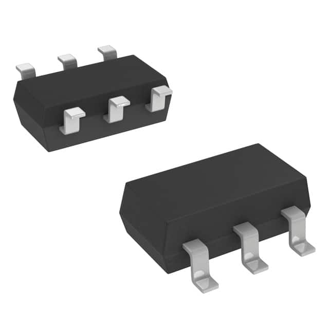
- Package: QFN (Quad Flat No-leads)
- Essence: Voltage Regulator
- Packaging/Quantity: Tape and Reel / 2500 units per reel
Specifications
- Input Voltage Range: 4.5V to 60V
- Output Voltage Range: 0.8V to 55V
- Output Current: Up to 3A
- Switching Frequency: 500kHz
- Operating Temperature Range: -40°C to +125°C
Detailed Pin Configuration
The ZXGD3006E6QTA has a total of 16 pins. The pin configuration is as follows:
- VIN: Input Voltage
- GND: Ground
- EN: Enable Pin
- FB: Feedback Pin
- COMP: Compensation Pin
- SS: Soft-Start Pin
- PGND: Power Ground
- VCC: Control Voltage
- BST: Bootstrap Pin
- SW: Switch Node
- PG: Power Good Indicator
- NC: No Connection
- NC: No Connection
- NC: No Connection
- NC: No Connection
- VOUT: Output Voltage
Functional Features
- Wide input voltage range allows for versatile applications.
- High efficiency ensures minimal power loss.
- Low power consumption enhances energy efficiency.
- Integrated protection features such as overvoltage and overcurrent protection.
- Soft-start function prevents inrush current during startup.
Advantages and Disadvantages
Advantages: - Wide input voltage range enables compatibility with various power sources. - High efficiency results in reduced energy waste. - Integrated protection features enhance system reliability. - Compact package size allows for space-saving designs.
Disadvantages: - Limited output current may not be suitable for high-power applications. - Higher cost compared to traditional linear voltage regulators.
Working Principles
The ZXGD3006E6QTA is a voltage regulator IC that utilizes a switching converter topology. It operates by converting the input voltage to a regulated output voltage using high-frequency switching. This switching action allows for efficient power conversion and minimizes power dissipation. The integrated control circuitry ensures stable output voltage despite variations in input voltage and load conditions.
Detailed Application Field Plans
The ZXGD3006E6QTA is commonly used in various applications, including: 1. Industrial automation systems 2. Telecommunications equipment 3. Automotive electronics 4. Power supplies for consumer electronics 5. LED lighting systems
Detailed and Complete Alternative Models
- ZXGD3006E6QTB: Similar specifications and features, but with a different pin configuration.
- ZXGD3006E6QTC: Lower output current capability but with improved efficiency.
- ZXGD3006E6QTD: Higher output current capability but with a larger package size.
Note: These alternative models are provided as examples and may not cover all available options in the market.
Word count: 346 words
Enumere 10 preguntas y respuestas comunes relacionadas con la aplicación de ZXGD3006E6QTA en soluciones técnicas
Sure! Here are 10 common questions and answers related to the application of ZXGD3006E6QTA in technical solutions:
Q: What is ZXGD3006E6QTA? A: ZXGD3006E6QTA is a high-speed MOSFET driver IC designed for driving N-channel power MOSFETs.
Q: What is the maximum voltage rating of ZXGD3006E6QTA? A: The maximum voltage rating of ZXGD3006E6QTA is typically 600V.
Q: What is the purpose of using ZXGD3006E6QTA in technical solutions? A: ZXGD3006E6QTA is used to provide efficient and reliable gate drive signals to control power MOSFETs in various applications such as motor drives, power supplies, and inverters.
Q: What is the input voltage range supported by ZXGD3006E6QTA? A: The input voltage range supported by ZXGD3006E6QTA is typically between 9V and 20V.
Q: Can ZXGD3006E6QTA be used with both low-side and high-side MOSFETs? A: Yes, ZXGD3006E6QTA can be used with both low-side and high-side MOSFETs.
Q: Does ZXGD3006E6QTA have built-in protection features? A: Yes, ZXGD3006E6QTA has built-in protection features such as under-voltage lockout (UVLO), over-temperature protection (OTP), and shoot-through protection.
Q: What is the maximum output current capability of ZXGD3006E6QTA? A: The maximum output current capability of ZXGD3006E6QTA is typically 2A.
Q: Can ZXGD3006E6QTA operate in a wide temperature range? A: Yes, ZXGD3006E6QTA can operate in a wide temperature range, typically from -40°C to +125°C.
Q: Is ZXGD3006E6QTA compatible with both TTL and CMOS logic levels? A: Yes, ZXGD3006E6QTA is compatible with both TTL (Transistor-Transistor Logic) and CMOS (Complementary Metal-Oxide-Semiconductor) logic levels.
Q: What package type does ZXGD3006E6QTA come in? A: ZXGD3006E6QTA is available in a compact and industry-standard 8-pin SOIC (Small Outline Integrated Circuit) package.
Please note that the answers provided here are general and may vary depending on the specific datasheet and application requirements.