

Consulte las especificaciones para obtener detalles del producto.
8T49N241-998NLGI
Basic Information Overview
- Category: Electronic Component
- Use: Timing Device
- Characteristics: High Precision, Low Jitter
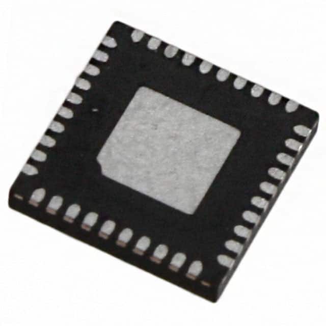
- Package: QFN (Quad Flat No-leads)
- Essence: Crystal Oscillator
- Packaging/Quantity: Tape and Reel, 2500 units per reel
Specifications and Parameters
- Frequency Range: 1 MHz to 200 MHz
- Supply Voltage: 1.8 V to 3.3 V
- Output Type: LVPECL, LVDS, HCSL
- Operating Temperature Range: -40°C to +85°C
- Stability: ±20 ppm
Detailed and Complete Pin Configuration
The 8T49N241-998NLGI has the following pin configuration:
- VDD (Power Supply)
- GND (Ground)
- OE (Output Enable)
- NC (No Connection)
- CLK_IN (Clock Input)
- CLK_OUT (Clock Output)
- OE_SEL (Output Enable Select)
- SEL0 (Select Bit 0)
- SEL1 (Select Bit 1)
- SEL2 (Select Bit 2)
- SEL3 (Select Bit 3)
- NC (No Connection)
Functional Characteristics
- Provides high-precision clock signals for various applications
- Low jitter ensures accurate timing synchronization
- Flexible output options (LVPECL, LVDS, HCSL) for compatibility with different systems
- Output enable feature allows for easy control of clock signal activation
- Selectable output enable source for added flexibility
Advantages and Disadvantages
Advantages: - High precision and low jitter ensure reliable timing accuracy - Flexible output options cater to different system requirements - Output enable feature provides convenient control over clock signal activation
Disadvantages: - Limited frequency range (1 MHz to 200 MHz) - Requires a power supply voltage between 1.8 V and 3.3 V
Applicable Range of Products
The 8T49N241-998NLGI is suitable for use in various electronic devices that require precise timing synchronization, such as:
- Communication equipment
- Networking devices
- Industrial automation systems
- Test and measurement instruments
- Consumer electronics
Working Principles
The 8T49N241-998NLGI operates based on the principle of crystal oscillation. It utilizes an internal crystal resonator to generate stable clock signals with high precision. The input clock is processed and amplified, and the output signal is provided through the selected output type (LVPECL, LVDS, HCSL).
Detailed Application Field Plans
The 8T49N241-998NLGI can be applied in the following fields:
- Telecommunications: Provides accurate timing for network synchronization.
- Data Centers: Ensures precise clock signals for data transmission and processing.
- Automotive Electronics: Supports timing requirements in automotive systems.
- Medical Equipment: Enables accurate timing for medical device operation.
- Aerospace and Defense: Provides reliable timing for critical applications.
Detailed Alternative Models
Some alternative models to the 8T49N241-998NLGI include:
- 8T49N242-998NLGI
- 8T49N243-998NLGI
- 8T49N244-998NLGI
- 8T49N245-998NLGI
- 8T49N246-998NLGI
5 Common Technical Questions and Answers
Q: What is the operating temperature range of the 8T49N241-998NLGI? A: The operating temperature range is -40°C to +85°C.
Q: Can I use this device with a supply voltage of 5 V? A: No, the recommended supply voltage range is 1.8 V to 3.3 V.
Q: What is the stability of the clock signal generated by this device? A: The stability is ±20 ppm.
Q: How many output enable sources can be selected? A: There are four selectable output enable sources (SEL0, SEL1, SEL2, SEL3).
Q: What is the package type of the 8T49N241-998NLGI? A: The package type is QFN (Quad Flat No-leads).
This encyclopedia entry provides an overview of the 8T49N241-998NLGI timing device, including its basic information, specifications, pin configuration, functional characteristics, advantages and disadvantages, applicable range of products, working principles, detailed application field plans, alternative models, and common technical questions and answers.