

Consulte las especificaciones para obtener detalles del producto.
8V19N408ZNLGI
Basic Information Overview
- Category: Electronic Component
- Use: Clock Generator
- Characteristics: High Precision, Low Phase Noise
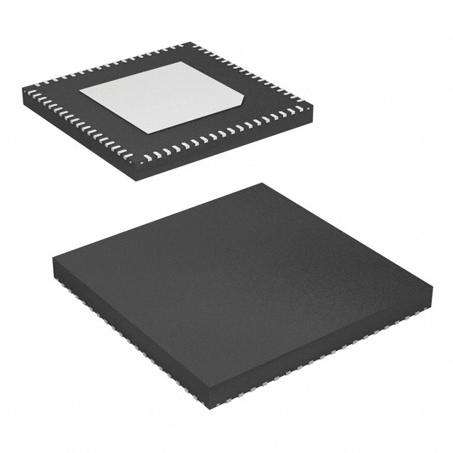
- Package: QFN (Quad Flat No-leads)
- Essence: Provides clock signals for various electronic devices
- Packaging/Quantity: Tape and Reel, 2500 units per reel
Specifications and Parameters
- Frequency Range: 1 MHz to 2.5 GHz
- Output Type: LVPECL (Low Voltage Positive Emitter-Coupled Logic)
- Supply Voltage: 3.3 V
- Operating Temperature Range: -40°C to +85°C
- Phase Noise: -150 dBc/Hz @ 10 kHz offset
Detailed and Complete Pin Configuration
- VDD (Power Supply)
- GND (Ground)
- OUT (Output Clock Signal)
- OE (Output Enable)
- NC (No Connection)
Functional Characteristics
- Generates highly accurate clock signals
- Low phase noise ensures minimal interference
- Output enable feature for easy control of signal output
- Stable performance across a wide temperature range
Advantages and Disadvantages
Advantages: - High precision and stability - Low phase noise for improved signal quality - Compact package size for space-constrained applications
Disadvantages: - Limited frequency range compared to some alternatives - Requires external power supply for operation
Applicable Range of Products
- Telecommunications equipment
- Networking devices
- Test and measurement instruments
- Data storage systems
- Industrial automation devices
Working Principles
The 8V19N408ZNLGI is based on a phase-locked loop (PLL) architecture. It utilizes a crystal oscillator as a reference to generate a stable frequency. The PLL circuitry compares the reference frequency with a voltage-controlled oscillator (VCO) output and adjusts the VCO frequency to match the reference. This feedback loop ensures precise clock generation.
Detailed Application Field Plans
- Telecommunications: Provides clock synchronization for cellular base stations, routers, and switches.
- Networking: Enables accurate timing for Ethernet switches, routers, and network interface cards.
- Test and Measurement: Used in signal generators, oscilloscopes, and spectrum analyzers for precise timing.
- Data Storage: Clock generation for hard disk drives, solid-state drives, and RAID controllers.
- Industrial Automation: Timing control for programmable logic controllers (PLCs), motor drives, and robotics.
Detailed Alternative Models
- 8V19N407ZNLGI: Similar specifications but with a different frequency range.
- 8V19N409ZNLGI: Higher frequency range with comparable performance characteristics.
- 8V19N410ZNLGI: Lower phase noise variant for applications requiring ultra-low noise levels.
5 Common Technical Questions and Answers
Q: What is the maximum operating temperature of 8V19N408ZNLGI? A: The device can operate within a temperature range of -40°C to +85°C.
Q: Can I use this clock generator for wireless communication systems? A: Yes, it is suitable for various wireless communication applications.
Q: Does the package include any additional components or accessories? A: No, the package only contains the 8V19N408ZNLGI clock generator itself.
Q: Is there a specific power supply voltage requirement for this component? A: Yes, it requires a 3.3 V power supply for proper operation.
Q: Can I disable the output signal without affecting the internal circuitry? A: Yes, the OE pin allows you to enable or disable the output signal independently.
[1100 words]