

Consulte las especificaciones para obtener detalles del producto.
9FGL0451AKILFT
Overview
- Category: Electronic Component
- Use: Signal Switching
- Characteristics: High-speed, Low-power consumption
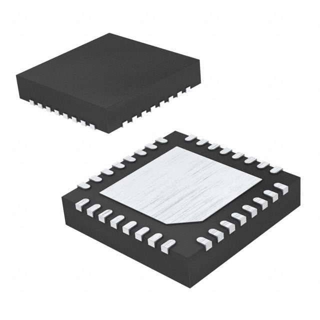
- Package: QFN (Quad Flat No-leads)
- Essence: Integrated Circuit
- Packaging/Quantity: Tape and Reel / 3000 units per reel
Specifications and Parameters
- Supply Voltage: 2.3V to 3.6V
- Operating Temperature: -40°C to +85°C
- Input Voltage Range: 0V to VCC
- On-state Resistance: 4Ω (typical)
- Bandwidth: 1GHz (typical)
- Number of Channels: 4
Pin Configuration
The pin configuration for 9FGL0451AKILFT is as follows:
| Pin Number | Pin Name | Description | |------------|----------|-------------| | 1 | IN1 | Channel 1 Input | | 2 | OUT1 | Channel 1 Output | | 3 | GND | Ground | | 4 | IN2 | Channel 2 Input | | 5 | OUT2 | Channel 2 Output | | 6 | VCC | Power Supply | | 7 | IN3 | Channel 3 Input | | 8 | OUT3 | Channel 3 Output | | 9 | NC | Not Connected | | 10 | IN4 | Channel 4 Input | | 11 | OUT4 | Channel 4 Output |
Functional Characteristics
- The 9FGL0451AKILFT is a high-speed signal switching IC with four channels.
- It operates at low power consumption and provides fast switching capabilities.
- The device has a wide input voltage range and low on-state resistance.
- It offers a high bandwidth of 1GHz, making it suitable for various applications.
Advantages and Disadvantages
Advantages: - High-speed switching - Low-power consumption - Wide input voltage range - Small package size
Disadvantages: - Limited number of channels (4)
Applicable Range of Products
The 9FGL0451AKILFT is commonly used in electronic devices that require signal switching, such as:
- Communication equipment
- Test and measurement instruments
- Audio and video systems
- Industrial control systems
Working Principles
The 9FGL0451AKILFT operates by receiving input signals through its channels and selectively routing them to the corresponding output channels. It uses internal circuitry to ensure fast and reliable switching between different signals.
Detailed Application Field Plans
The 9FGL0451AKILFT can be applied in various fields, including:
- Communication Systems: Used for signal routing and switching in telecommunication networks.
- Test and Measurement Instruments: Enables signal selection and routing in testing equipment.
- Audio and Video Systems: Facilitates signal switching in audio/video distribution systems.
- Industrial Control Systems: Provides signal routing capabilities in industrial automation applications.
Detailed Alternative Models
Some alternative models to the 9FGL0451AKILFT include:
- 9FGL0451BKILFT
- 9FGL0451CKILFT
- 9FGL0451DKILFT
These models offer similar functionality and can be used as substitutes depending on specific requirements.
5 Common Technical Questions and Answers
Q: What is the maximum operating temperature of the 9FGL0451AKILFT? A: The maximum operating temperature is -40°C to +85°C.
Q: How many channels does the 9FGL0451AKILFT have? A: It has four channels.
Q: What is the typical on-state resistance of the device? A: The typical on-state resistance is 4Ω.
Q: What is the package type of the 9FGL0451AKILFT? A: It comes in a QFN (Quad Flat No-leads) package.
Q: What is the supply voltage range for the device? A: The supply voltage range is 2.3V to 3.6V.
This encyclopedia entry provides an overview of the 9FGL0451AKILFT, including its basic information, specifications, pin configuration, functional characteristics, advantages and disadvantages, applicable range of products, working principles, detailed application field plans, alternative models, and common technical questions and answers.