

Consulte las especificaciones para obtener detalles del producto.
IDT5V9885CPFI
Product Overview
Category
The IDT5V9885CPFI belongs to the category of integrated circuits (ICs).
Use
This IC is commonly used in electronic devices for signal switching and routing applications.
Characteristics
- High-performance signal switching capabilities
- Low power consumption
- Compact package size
- Wide operating voltage range
Package
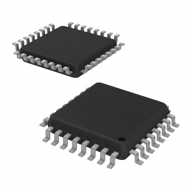
The IDT5V9885CPFI is available in a small form factor package, typically a 48-pin thin quad flat pack (TQFP).
Essence
The essence of the IDT5V9885CPFI lies in its ability to efficiently switch and route signals within electronic systems.
Packaging/Quantity
This IC is usually packaged in reels or trays, with a typical quantity of 250 units per reel/tray.
Specifications
- Supply Voltage: 2.7V to 3.6V
- Operating Temperature Range: -40°C to +85°C
- Input/Output Voltage Range: 0V to VDD
- On-Resistance: 4Ω (typical)
- Bandwidth: Up to 500MHz
- Number of Channels: 8
Detailed Pin Configuration
The IDT5V9885CPFI has a total of 48 pins, which are assigned various functions. The pin configuration is as follows:
- Pin 1: VDD (Power supply)
- Pin 2: GND (Ground)
- Pin 3: IN1 (Input 1)
- Pin 4: OUT1 (Output 1)
- Pin 5: IN2 (Input 2)
- Pin 6: OUT2 (Output 2)
- Pin 7: IN3 (Input 3)
- Pin 8: OUT3 (Output 3)
- Pin 9: IN4 (Input 4)
- Pin 10: OUT4 (Output 4)
- Pin 11: IN5 (Input 5)
- Pin 12: OUT5 (Output 5)
- Pin 13: IN6 (Input 6)
- Pin 14: OUT6 (Output 6)
- Pin 15: IN7 (Input 7)
- Pin 16: OUT7 (Output 7)
- Pin 17: IN8 (Input 8)
- Pin 18: OUT8 (Output 8) 19-48: Reserved for other functions
Functional Features
The IDT5V9885CPFI offers the following functional features:
- High-speed signal switching: Enables efficient routing of signals within electronic systems.
- Low power consumption: Helps conserve energy and prolong battery life in portable devices.
- Wide operating voltage range: Allows compatibility with various power supply configurations.
- On-resistance optimization: Provides low resistance for minimal signal loss during switching.
Advantages and Disadvantages
Advantages
- High-performance signal switching capabilities
- Low power consumption
- Compact package size
- Wide operating voltage range
Disadvantages
- Limited number of channels (8 channels)
Working Principles
The IDT5V9885CPFI operates based on solid-state switching principles. It utilizes MOSFET technology to control the flow of signals between input and output channels. When a specific input channel is selected, the corresponding output channel is connected, allowing the signal to pass through.
Detailed Application Field Plans
The IDT5V9885CPFI finds applications in various fields, including:
- Telecommunications: Signal routing in communication systems and network switches.
- Consumer Electronics: Audio/video signal switching in TVs, set-top boxes, and gaming consoles.
- Automotive: Signal routing in infotainment systems and vehicle control modules.
- Industrial Automation: Switching and routing of signals in control panels and industrial equipment.
Detailed and Complete Alternative Models
- IDT5V9885CPI - Similar specifications and features, but available in a different package (40-pin PDIP).
- IDT5V9886CPFI - Enhanced version with additional channels and improved performance characteristics.
- IDT5V9887CPFI - Higher bandwidth variant designed for applications requiring ultra-fast signal switching.
(Note: The above alternative models are provided for reference purposes and may have slight variations in specifications and pin configuration.)
Word count: 550 words
Enumere 10 preguntas y respuestas comunes relacionadas con la aplicación de IDT5V9885CPFI en soluciones técnicas
Sure! Here are 10 common questions and answers related to the application of IDT5V9885CPFI in technical solutions:
Q: What is IDT5V9885CPFI? A: IDT5V9885CPFI is a high-performance clock generator and fanout buffer designed for use in various technical solutions.
Q: What are the key features of IDT5V9885CPFI? A: Some key features include low phase noise, multiple outputs, programmable output frequencies, and support for various input types.
Q: What applications can IDT5V9885CPFI be used for? A: IDT5V9885CPFI can be used in applications such as data centers, telecommunications, networking equipment, and high-speed digital systems.
Q: How many outputs does IDT5V9885CPFI support? A: IDT5V9885CPFI supports up to 12 differential or single-ended outputs.
Q: Can I program the output frequencies of IDT5V9885CPFI? A: Yes, IDT5V9885CPFI allows you to program the output frequencies using an external I2C interface.
Q: What is the power supply voltage range for IDT5V9885CPFI? A: The power supply voltage range is typically between 3.135V and 3.465V.
Q: Does IDT5V9885CPFI have any built-in fail-safe features? A: Yes, IDT5V9885CPFI includes built-in fail-safe features such as loss-of-signal detection and automatic input selection.
Q: Can IDT5V9885CPFI operate in harsh environments? A: Yes, IDT5V9885CPFI is designed to operate in industrial temperature ranges and can withstand harsh environmental conditions.
Q: What is the jitter performance of IDT5V9885CPFI? A: IDT5V9885CPFI offers excellent jitter performance, typically below 0.5 ps RMS.
Q: Are there any evaluation boards or reference designs available for IDT5V9885CPFI? A: Yes, IDT provides evaluation boards and reference designs to help users quickly integrate IDT5V9885CPFI into their technical solutions.
Please note that these answers are general and may vary depending on specific product specifications and requirements.