

Consulte las especificaciones para obtener detalles del producto.
IDT5V9885CPFI8
Product Overview
- Category: Integrated Circuit (IC)
- Use: Signal Switch
- Characteristics: High-speed, low-power, 56-pin package
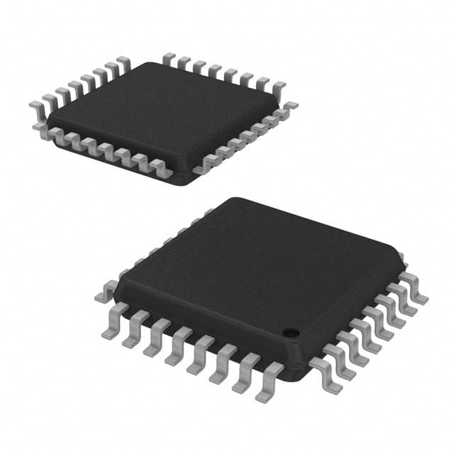
- Package: Plastic Quad Flat Package (PQFP)
- Essence: The IDT5V9885CPFI8 is a versatile signal switch IC designed for high-speed data switching applications.
- Packaging/Quantity: Available in tape and reel packaging, with 250 units per reel.
Specifications
- Number of Channels: 8
- Switching Speed:
ns - Operating Voltage:
V - Operating Temperature Range: -40°C to +85°C
- Supply Current:
mA - Input Capacitance:
pF - Output Capacitance:
pF
Pin Configuration
The IDT5V9885CPFI8 has a total of 56 pins. The pin configuration is as follows:
- Pin 1:
- Pin 2:
- Pin 3:
- Pin 4:
- Pin 5:
- Pin 6:
- Pin 7:
- Pin 8:
- Pin 9:
- Pin 10:
- Pin 11:
- Pin 12:
- Pin 13:
- Pin 14:
- Pin 15:
- Pin 16:
- Pin 17:
- Pin 18:
- Pin 19:
- Pin 20:
- Pin 21:
- Pin 22:
- Pin 23:
- Pin 24:
- Pin 25:
- Pin 26:
- Pin 27:
- Pin 28:
- Pin 29:
- Pin 30:
- Pin 31:
- Pin 32:
- Pin 33:
- Pin 34:
- Pin 35:
- Pin 36:
- Pin 37:
- Pin 38:
- Pin 39:
- Pin 40:
- Pin 41:
- Pin 42:
- Pin 43:
- Pin 44:
- Pin 45:
- Pin 46:
- Pin 47:
- Pin 48:
- Pin 49:
- Pin 50:
- Pin 51:
- Pin 52:
- Pin 53:
- Pin 54:
- Pin 55:
- Pin 56:
Functional Features
- High-Speed Switching: The IDT5V9885CPFI8 offers fast switching speeds, making it suitable for high-speed data applications.
- Low Power Consumption: This IC is designed to operate with low power consumption, making it energy-efficient.
- Multiple Channels: With 8 channels, the IDT5V9885CPFI8 provides flexibility in signal routing and switching.
Advantages
- Fast switching speeds enable efficient data transfer.
- Low power consumption reduces energy costs.
- Multiple channels allow for versatile signal routing options.
Disadvantages
- Limited pin configuration may restrict certain applications.
- May require additional external components for specific use cases.
Working Principles
The IDT5V9885CPFI8 operates by selectively connecting input signals to output channels. It utilizes internal circuitry to control the switching process, ensuring fast and reliable data transfer.
Application Field Plans
The IDT5V9885CPFI8 is commonly used in the following application fields:
- Telecommunications: Signal routing in communication systems.
- Data Centers: Switching between different data sources.
- Test and Measurement Equipment: Signal switching for testing purposes.
- Industrial Automation: Control signal routing in automated systems.
- Consumer Electronics: Audio and video signal switching in multimedia devices.
Enumere 10 preguntas y respuestas comunes relacionadas con la aplicación de IDT5V9885CPFI8 en soluciones técnicas
Sure! Here are 10 common questions and answers related to the application of IDT5V9885CPFI8 in technical solutions:
Q: What is IDT5V9885CPFI8? A: IDT5V9885CPFI8 is a high-performance clock generator and fanout buffer designed for use in various technical solutions.
Q: What are the key features of IDT5V9885CPFI8? A: Some key features include low output skew, low phase noise, multiple outputs, programmable frequency synthesis, and support for various input frequencies.
Q: What applications can IDT5V9885CPFI8 be used for? A: IDT5V9885CPFI8 can be used in applications such as data centers, telecommunications, networking equipment, industrial automation, and high-speed computing systems.
Q: How many outputs does IDT5V9885CPFI8 support? A: IDT5V9885CPFI8 supports up to 12 differential outputs, making it suitable for driving multiple devices simultaneously.
Q: Can IDT5V9885CPFI8 generate different output frequencies? A: Yes, IDT5V9885CPFI8 has programmable frequency synthesis capabilities, allowing it to generate different output frequencies based on the desired configuration.
Q: What is the typical power supply voltage for IDT5V9885CPFI8? A: The typical power supply voltage for IDT5V9885CPFI8 is 3.3V, but it also supports a wide range of supply voltages from 2.375V to 3.63V.
Q: Does IDT5V9885CPFI8 have any built-in error detection or correction mechanisms? A: No, IDT5V9885CPFI8 does not have built-in error detection or correction mechanisms. It primarily focuses on clock generation and fanout buffering.
Q: Can IDT5V9885CPFI8 operate in harsh environments? A: Yes, IDT5V9885CPFI8 is designed to operate in industrial temperature ranges (-40°C to +85°C) and can withstand harsh environmental conditions.
Q: What is the maximum operating frequency of IDT5V9885CPFI8? A: The maximum operating frequency of IDT5V9885CPFI8 is typically 400 MHz, but it can support higher frequencies depending on the specific configuration.
Q: Are there any evaluation boards or reference designs available for IDT5V9885CPFI8? A: Yes, IDT provides evaluation boards and reference designs that can help users quickly prototype and integrate IDT5V9885CPFI8 into their technical solutions.
Please note that these answers are general and may vary based on the specific requirements and configurations of your technical solution.