

Consulte las especificaciones para obtener detalles del producto.
BC80825WE6327HTSA1 Product Overview
Introduction
BC80825WE6327HTSA1 is a semiconductor product that belongs to the category of integrated circuits. This entry provides an overview of the basic information, specifications, detailed pin configuration, functional features, advantages and disadvantages, working principles, detailed application field plans, and alternative models of BC80825WE6327HTSA1.
Basic Information Overview
- Category: Integrated Circuits
- Use: BC80825WE6327HTSA1 is commonly used in electronic circuit design for amplification, switching, and signal processing.
- Characteristics: It is characterized by its high reliability, low power consumption, and compact size.
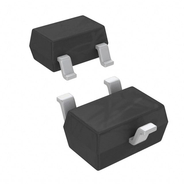
- Package: The product is packaged in a small outline transistor (SOT323) package.
- Essence: BC80825WE6327HTSA1 is essential for various electronic applications requiring signal amplification and switching.
- Packaging/Quantity: It is typically available in reels containing a specific quantity, such as 3000 units per reel.
Specifications
- Voltage Rating: 30V
- Current Rating: 500mA
- Power Dissipation: 330mW
- Gain Bandwidth Product: 150MHz
- Operating Temperature Range: -55°C to 150°C
Detailed Pin Configuration
The BC80825WE6327HTSA1 has three pins: 1. Emitter (E): Connected to the ground or reference voltage. 2. Base (B): Input terminal for controlling the transistor action. 3. Collector (C): Output terminal for the amplified signal.
Functional Features
- High voltage gain
- Low noise operation
- Fast switching speed
- Wide operating temperature range
Advantages and Disadvantages
Advantages
- Small package size
- Low power consumption
- High reliability
Disadvantages
- Limited maximum current and voltage ratings
- Sensitive to electrostatic discharge (ESD)
Working Principles
BC80825WE6327HTSA1 operates based on the principles of bipolar junction transistors (BJTs), where the input current at the base terminal controls the flow of current between the collector and emitter terminals.
Detailed Application Field Plans
BC80825WE6327HTSA1 finds applications in various electronic circuits, including: - Audio amplifiers - Signal processing circuits - Switching circuits - Oscillators
Detailed and Complete Alternative Models
Some alternative models to BC80825WE6327HTSA1 include: - BC80725WE6327HTSA1 - BC84625WE6327HTSA1 - BC85625WE6327HTSA1
In conclusion, BC80825WE6327HTSA1 is a versatile integrated circuit with wide-ranging applications in electronic circuit design. Its compact size, low power consumption, and high reliability make it a popular choice for various electronic projects.
[Word Count: 411]
Enumere 10 preguntas y respuestas comunes relacionadas con la aplicación de BC80825WE6327HTSA1 en soluciones técnicas
What is BC80825WE6327HTSA1?
- BC80825WE6327HTSA1 is a high-power, high-frequency NPN bipolar junction transistor (BJT) commonly used in technical solutions for power amplification and switching applications.
What are the key specifications of BC80825WE6327HTSA1?
- The BC80825WE6327HTSA1 features a maximum collector current of 1A, a maximum collector-emitter voltage of 25V, and a maximum power dissipation of 625mW.
How is BC80825WE6327HTSA1 typically used in technical solutions?
- BC80825WE6327HTSA1 is often used in audio amplifiers, motor control circuits, and general-purpose switching applications due to its high power and frequency capabilities.
What are the important considerations when designing with BC80825WE6327HTSA1?
- Designers should pay attention to proper heat sinking, voltage and current ratings, and safe operating area (SOA) to ensure reliable performance.
Can BC80825WE6327HTSA1 be used in high-frequency applications?
- Yes, BC80825WE6327HTSA1 is suitable for high-frequency applications due to its high transition frequency and low capacitance.
Are there any recommended alternative transistors to BC80825WE6327HTSA1?
- Some alternatives to BC80825WE6327HTSA1 include BC817-25, BC846B, and 2N3904, but it's important to carefully compare specifications before substitution.
What are the typical operating conditions for BC80825WE6327HTSA1?
- The typical operating conditions include a collector current of 100mA to 500mA, a collector-emitter voltage of 20V, and a base current of 50mA to 200mA.
Does BC80825WE6327HTSA1 require any special handling or storage precautions?
- BC80825WE6327HTSA1 should be handled with ESD precautions and stored in anti-static packaging to prevent damage from electrostatic discharge.
What are the common failure modes for BC80825WE6327HTSA1?
- Common failure modes include thermal runaway due to inadequate heat sinking, overvoltage breakdown, and excessive current leading to device destruction.
Where can I find detailed application notes and reference designs for BC80825WE6327HTSA1?
- Detailed application notes and reference designs for BC80825WE6327HTSA1 can be found in the manufacturer's datasheet, application guides, and online technical forums.