

Consulte las especificaciones para obtener detalles del producto.
5AGXMA5G4F31I5
Basic Information Overview
- Category: Integrated Circuit (IC)
- Use: Programmable Logic Device (PLD)
- Characteristics: High-performance, low-power consumption, reprogrammable
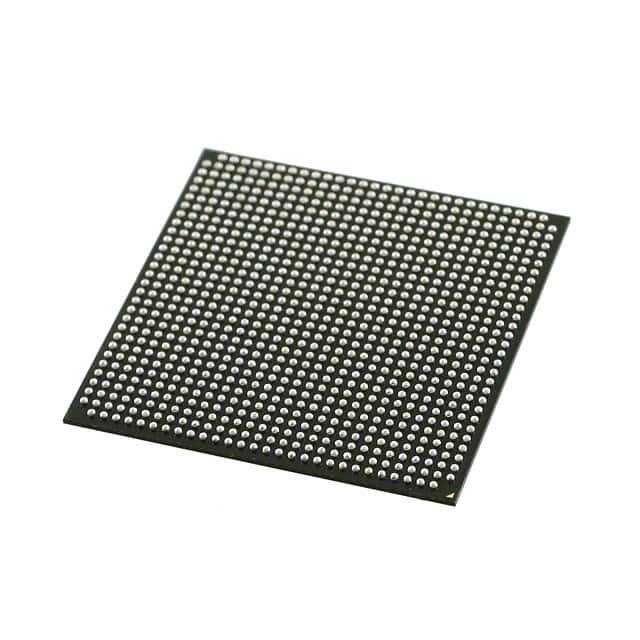
- Package: BGA (Ball Grid Array)
- Essence: FPGA (Field-Programmable Gate Array)
- Packaging/Quantity: Single unit
Specifications
- Manufacturer: Intel Corporation
- Family: Arria® V GX
- Device: 5AGXMA5G4F31I5
- Logic Elements: 462,000
- Embedded Memory: 8,192 Kbits
- DSP Blocks: 360
- Maximum User I/O Pins: 1,040
- Operating Voltage: 1.2V
- Operating Temperature: -40°C to +100°C
Detailed Pin Configuration
The detailed pin configuration for 5AGXMA5G4F31I5 can be found in the manufacturer's datasheet.
Functional Features
- High-speed performance with advanced architecture
- Low power consumption for energy-efficient applications
- Reprogrammable nature allows for flexibility and design iterations
- Support for various communication protocols and interfaces
- On-chip memory resources for efficient data storage and retrieval
- Built-in digital signal processing capabilities for signal manipulation
Advantages
- Versatile and adaptable to a wide range of applications
- Faster time-to-market due to reprogrammability
- Lower development costs compared to custom ASICs
- High-performance computing capabilities
- Integration of multiple functions into a single device
Disadvantages
- Higher cost compared to traditional fixed-function ICs
- Limited availability of alternative models from other manufacturers
- Steeper learning curve for programming and utilizing FPGA technology
- Increased complexity in design and verification process
Working Principles
5AGXMA5G4F31I5 is based on FPGA technology, which allows users to configure the device's logic functions and interconnections according to their specific requirements. The device consists of an array of programmable logic blocks interconnected by programmable routing resources. These logic blocks can be configured to perform various functions, such as arithmetic operations, data processing, and control tasks. The configuration is done using a hardware description language (HDL) and is stored in non-volatile memory within the device.
Detailed Application Field Plans
- High-performance computing systems
- Digital signal processing applications
- Communication and networking equipment
- Industrial automation and control systems
- Aerospace and defense electronics
- Medical imaging and diagnostic devices
Detailed and Complete Alternative Models
- Xilinx Virtex UltraScale+ series
- Lattice Semiconductor ECP5 series
- Microsemi SmartFusion2 series
- QuickLogic PolarPro series
- Actel ProASIC3 series
(Note: This list is not exhaustive and alternative models may vary based on specific requirements and availability.)
This entry provides an overview of the 5AGXMA5G4F31I5 programmable logic device, including its basic information, specifications, pin configuration, functional features, advantages, disadvantages, working principles, application field plans, and alternative models.
Enumere 10 preguntas y respuestas comunes relacionadas con la aplicación de 5AGXMA5G4F31I5 en soluciones técnicas
Sure! Here are 10 common questions and answers related to the application of 5AGXMA5G4F31I5 in technical solutions:
Q: What is the 5AGXMA5G4F31I5 FPGA used for? A: The 5AGXMA5G4F31I5 FPGA is commonly used for implementing complex digital logic circuits in various technical solutions.
Q: What are some key features of the 5AGXMA5G4F31I5 FPGA? A: Some key features include high-performance processing capabilities, low power consumption, large programmable logic capacity, and support for various communication protocols.
Q: How can the 5AGXMA5G4F31I5 FPGA be programmed? A: The 5AGXMA5G4F31I5 FPGA can be programmed using hardware description languages (HDLs) such as VHDL or Verilog, or through graphical programming tools like Quartus Prime.
Q: What applications can benefit from using the 5AGXMA5G4F31I5 FPGA? A: The 5AGXMA5G4F31I5 FPGA can be used in a wide range of applications including telecommunications, aerospace, automotive, industrial automation, and high-performance computing.
Q: Can the 5AGXMA5G4F31I5 FPGA interface with other components or devices? A: Yes, the 5AGXMA5G4F31I5 FPGA supports various interfaces such as PCIe, Ethernet, USB, SPI, I2C, and more, allowing seamless integration with other components or devices.
Q: What is the maximum operating frequency of the 5AGXMA5G4F31I5 FPGA? A: The maximum operating frequency of the 5AGXMA5G4F31I5 FPGA is typically specified in the datasheet and depends on the specific design and implementation.
Q: Can the 5AGXMA5G4F31I5 FPGA be reprogrammed after deployment? A: Yes, the 5AGXMA5G4F31I5 FPGA can be reprogrammed multiple times, allowing for flexibility and updates to the functionality of the system.
Q: Are there any development kits available for the 5AGXMA5G4F31I5 FPGA? A: Yes, Intel (formerly Altera) provides development kits that include the necessary hardware and software tools to get started with designing and programming the 5AGXMA5G4F31I5 FPGA.
Q: What kind of support is available for the 5AGXMA5G4F31I5 FPGA? A: Intel offers technical documentation, application notes, online forums, and customer support to assist users with any questions or issues related to the 5AGXMA5G4F31I5 FPGA.
Q: Can the 5AGXMA5G4F31I5 FPGA be used in safety-critical applications? A: Yes, the 5AGXMA5G4F31I5 FPGA can be used in safety-critical applications, but it requires proper design practices, verification, and validation to ensure compliance with relevant safety standards.