Consulte las especificaciones para obtener detalles del producto.

5CGXBC5C6F23C7N
Product Overview
Category
The 5CGXBC5C6F23C7N belongs to the category of Field Programmable Gate Arrays (FPGAs).
Use
FPGAs are integrated circuits that can be programmed and reprogrammed to perform various digital functions. The 5CGXBC5C6F23C7N is specifically designed for high-performance applications requiring complex logic functions.
Characteristics
- High-performance FPGA with advanced features
- Large number of programmable logic elements
- High-speed transceivers for data communication
- On-chip memory resources
- Support for various I/O standards
- Low power consumption
Package
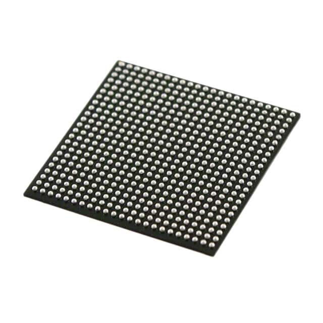
The 5CGXBC5C6F23C7N is available in a compact package, suitable for surface mount technology (SMT) assembly.
Essence
The essence of the 5CGXBC5C6F23C7N lies in its ability to provide flexible and customizable digital logic functionality, allowing designers to implement complex systems on a single chip.
Packaging/Quantity
The 5CGXBC5C6F23C7N is typically packaged in trays or reels, with a quantity of multiple units per package.
Specifications
- Logic Elements: 5,600
- Embedded Memory: Up to 1,638 Kbits
- Transceivers: Up to 24 channels
- I/O Standards: LVCMOS, LVTTL, SSTL, HSTL, LVDS, etc.
- Operating Voltage: 1.2V
- Operating Temperature Range: -40°C to 100°C
- Package Type: BGA (Ball Grid Array)
- Package Pins: 484
Detailed Pin Configuration
The 5CGXBC5C6F23C7N has a total of 484 pins, each serving a specific purpose in the FPGA's operation. The pin configuration includes dedicated input/output pins, clock inputs, power supply pins, and configuration interface pins.
For a detailed pin configuration diagram, please refer to the datasheet provided by the manufacturer.
Functional Features
High-Performance Computing
The 5CGXBC5C6F23C7N offers a large number of logic elements, allowing for the implementation of complex computational tasks with high efficiency.
Flexible I/O Interfaces
With support for various I/O standards, the FPGA can interface with a wide range of external devices, enabling seamless integration into different systems.
High-Speed Data Communication
The transceivers integrated into the 5CGXBC5C6F23C7N enable fast and reliable data communication between the FPGA and other components, making it suitable for applications requiring high-speed data transfer.
On-Chip Memory Resources
The embedded memory blocks provide additional storage capacity within the FPGA, reducing the need for external memory components and enhancing overall system performance.
Advantages and Disadvantages
Advantages
- Flexibility and reprogrammability
- High-performance computing capabilities
- Support for various I/O standards
- On-chip memory resources reduce external component requirements
- Low power consumption compared to alternative solutions
Disadvantages
- Higher cost compared to traditional fixed-function integrated circuits
- Steeper learning curve for programming and utilizing FPGAs effectively
Working Principles
The 5CGXBC5C6F23C7N operates based on the principles of configurable logic. It consists of an array of programmable logic elements interconnected through configurable routing resources. By programming the interconnections and logic functions, designers can create custom digital circuits tailored to their specific application requirements.
Detailed Application Field Plans
The 5CGXBC5C6F23C7N finds applications in various fields, including:
- Telecommunications: High-speed data processing and communication systems.
- Industrial Automation: Control systems for manufacturing processes and robotics.
- Aerospace and Defense: Radar signal processing, image recognition, and secure communications.
- Medical Devices: Real-time data acquisition and processing in medical imaging equipment.
- Automotive: Advanced driver assistance systems (ADAS) and infotainment systems.
Detailed and Complete Alternative Models
- 5CGXBC5C6F27C7N
- 5CGXBC5C6F31C7N
- 5CGXBC5C6F35C7N
- 5CGXBC5C6F40C7N
These alternative models offer similar features and capabilities to the 5CGXBC5C6F23C7N, with variations in logic capacity, memory resources, and transceiver channels.
Note: Please refer to the manufacturer's documentation for detailed specifications of each alternative model.
Word count: 660 words
Enumere 10 preguntas y respuestas comunes relacionadas con la aplicación de 5CGXBC5C6F23C7N en soluciones técnicas
Sure! Here are 10 common questions and answers related to the application of 5CGXBC5C6F23C7N in technical solutions:
Q: What is the 5CGXBC5C6F23C7N? A: The 5CGXBC5C6F23C7N is a specific model of Field Programmable Gate Array (FPGA) manufactured by Intel.
Q: What are the key features of the 5CGXBC5C6F23C7N? A: The 5CGXBC5C6F23C7N offers high-performance, low-power consumption, large capacity, and a wide range of I/O interfaces.
Q: What are some typical applications for the 5CGXBC5C6F23C7N? A: The 5CGXBC5C6F23C7N can be used in various applications such as telecommunications, industrial automation, automotive electronics, and high-performance computing.
Q: How does the 5CGXBC5C6F23C7N differ from other FPGAs? A: The 5CGXBC5C6F23C7N stands out due to its high logic density, advanced DSP capabilities, and support for high-speed serial communication protocols.
Q: Can the 5CGXBC5C6F23C7N be reprogrammed after deployment? A: Yes, the 5CGXBC5C6F23C7N is a field-programmable device, meaning it can be reconfigured even after being deployed in a system.
Q: What development tools are available for programming the 5CGXBC5C6F23C7N? A: Intel provides Quartus Prime software, which is widely used for designing and programming FPGAs, including the 5CGXBC5C6F23C7N.
Q: Can the 5CGXBC5C6F23C7N interface with other components or devices? A: Yes, the 5CGXBC5C6F23C7N supports various I/O standards, such as LVDS, PCIe, Ethernet, USB, and more, allowing it to interface with a wide range of components and devices.
Q: What are the power requirements for the 5CGXBC5C6F23C7N? A: The power requirements vary depending on the specific configuration and usage scenario. It is recommended to refer to the datasheet for detailed information.
Q: Are there any known limitations or considerations when using the 5CGXBC5C6F23C7N? A: Some considerations include thermal management due to high-performance operation, potential signal integrity issues at high frequencies, and the need for proper design practices to optimize performance.
Q: Where can I find additional resources and support for the 5CGXBC5C6F23C7N? A: Intel's website provides comprehensive documentation, application notes, reference designs, and a community forum where you can find additional resources and seek support for the 5CGXBC5C6F23C7N.
Please note that the answers provided here are general and may vary based on specific requirements and use cases.

