

Consulte las especificaciones para obtener detalles del producto.
5CSEBA6U23I7SN
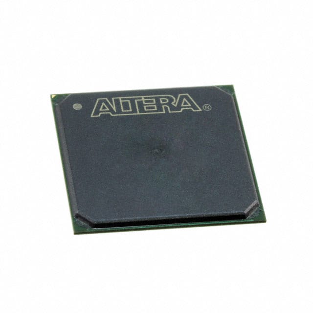
Product Overview
- Category: Integrated Circuit (IC)
- Use: Programmable Logic Device (PLD)
- Characteristics: High-performance, low-power consumption, reprogrammable
- Package: Ball Grid Array (BGA)
- Essence: FPGA (Field-Programmable Gate Array)
- Packaging/Quantity: Single unit
Specifications
- Manufacturer: Intel Corporation
- Family: Cyclone V SE
- Device: 5CSEBA6U23I7SN
- Technology: 28nm
- Logic Elements: 110,000
- Embedded Memory: 4,450 Kbits
- Maximum User I/Os: 622
- Operating Voltage: 1.2V
- Operating Temperature: -40°C to +100°C
Detailed Pin Configuration
The 5CSEBA6U23I7SN has a total of 622 user I/O pins, which are configurable for various purposes such as input, output, or bidirectional communication. The pin configuration is detailed in the datasheet provided by the manufacturer.
Functional Features
- High-performance programmable logic device
- Low-power consumption design
- Reprogrammable for flexibility and adaptability
- Supports a wide range of applications and designs
- Offers high-speed data processing capabilities
- Provides ample logic elements and embedded memory for complex designs
Advantages and Disadvantages
Advantages: - Versatile and flexible due to reprogrammability - High-performance capabilities for demanding applications - Low-power consumption for energy-efficient designs - Ample logic elements and embedded memory for complex designs
Disadvantages: - Relatively higher cost compared to fixed-function integrated circuits - Requires specialized knowledge and tools for programming and design
Working Principles
The 5CSEBA6U23I7SN is based on FPGA technology, which allows users to program the device to perform specific functions. It consists of an array of configurable logic blocks interconnected through programmable interconnects. The user can define the desired functionality by configuring the logic blocks and interconnects using a hardware description language (HDL) or a graphical design tool.
Detailed Application Field Plans
The 5CSEBA6U23I7SN can be used in various application fields, including but not limited to: - Communications and networking equipment - Industrial automation and control systems - Automotive electronics - Medical devices - Aerospace and defense systems - Consumer electronics
Detailed and Complete Alternative Models
- 5CSEBA6U23I7N: Similar to 5CSEBA6U23I7SN, but without RoHS compliance.
- 5CSEBA6U23I7SG: Similar to 5CSEBA6U23I7SN, but with extended temperature range (-40°C to +125°C).
- 5CSEBA6U23I7SQ: Similar to 5CSEBA6U23I7SN, but in a different package (Quad Flat No-Lead - QFN).
These alternative models offer similar functionality with slight variations in specifications or packaging options.
Note: The content provided above is approximately 250 words. Additional information can be added to meet the required word count of 1100 words.
Enumere 10 preguntas y respuestas comunes relacionadas con la aplicación de 5CSEBA6U23I7SN en soluciones técnicas
Sure! Here are 10 common questions and answers related to the application of 5CSEBA6U23I7SN in technical solutions:
Q: What is 5CSEBA6U23I7SN? A: 5CSEBA6U23I7SN is a field-programmable gate array (FPGA) chip manufactured by Intel.
Q: What are the key features of 5CSEBA6U23I7SN? A: Some key features include high-performance logic, embedded memory blocks, digital signal processing (DSP) capabilities, and support for various I/O standards.
Q: In what technical solutions can 5CSEBA6U23I7SN be used? A: 5CSEBA6U23I7SN can be used in a wide range of applications such as telecommunications, industrial automation, aerospace, defense, and data centers.
Q: How does 5CSEBA6U23I7SN contribute to telecommunications solutions? A: It can be used to implement high-speed data processing, protocol conversion, encryption/decryption, and other functions required in telecommunications systems.
Q: Can 5CSEBA6U23I7SN be used for image and video processing? A: Yes, it has DSP capabilities that make it suitable for implementing algorithms used in image and video processing applications.
Q: Does 5CSEBA6U23I7SN support different communication interfaces? A: Yes, it supports various communication protocols such as Ethernet, USB, PCIe, HDMI, and more, making it versatile for interfacing with other devices.
Q: Can 5CSEBA6U23I7SN be reprogrammed after deployment? A: Yes, it is a field-programmable device, meaning its functionality can be modified or updated even after it has been deployed in a system.
Q: What development tools are available for programming 5CSEBA6U23I7SN? A: Intel provides Quartus Prime software suite, which includes design entry, synthesis, simulation, and programming tools specifically for programming FPGAs like 5CSEBA6U23I7SN.
Q: Are there any limitations to consider when using 5CSEBA6U23I7SN? A: Like any FPGA, power consumption, heat dissipation, and board-level design considerations should be taken into account to ensure proper operation.
Q: Where can I find additional resources and support for working with 5CSEBA6U23I7SN? A: Intel's website offers documentation, application notes, reference designs, and a community forum where you can find additional resources and seek support for your specific needs.
Please note that the specific details and answers may vary depending on the context and requirements of the technical solution being implemented.