

Consulte las especificaciones para obtener detalles del producto.
5SGSMD3E2H29C2L
Product Overview
Category
The 5SGSMD3E2H29C2L belongs to the category of Field Programmable Gate Arrays (FPGAs).
Use
This FPGA is primarily used in digital logic circuits for various applications such as telecommunications, automotive, aerospace, and industrial control systems.
Characteristics
- High-performance programmable logic device
- Offers high-speed data processing capabilities
- Provides flexibility for customization and reconfiguration
- Supports complex algorithms and computations
- Low power consumption
- Reliable and durable
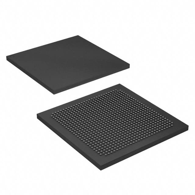
Package
The 5SGSMD3E2H29C2L comes in a compact package that ensures easy integration into electronic systems. It is designed to be mounted on printed circuit boards (PCBs) using surface mount technology (SMT).
Essence
The essence of the 5SGSMD3E2H29C2L lies in its ability to provide a versatile and efficient solution for implementing complex digital logic functions in electronic systems.
Packaging/Quantity
This FPGA is typically packaged in trays or reels, depending on the manufacturer's specifications. The quantity per package may vary, but it is commonly available in quantities suitable for both prototyping and production purposes.
Specifications
- Logic Elements: 220,000
- Embedded Memory: 8,000 Kbits
- Maximum User I/Os: 1,040
- DSP Blocks: 744
- Clock Management Tiles: 16
- Transceivers: 24
- Operating Voltage: 1.2V
- Operating Temperature Range: -40°C to +100°C
Detailed Pin Configuration
The pin configuration of the 5SGSMD3E2H29C2L FPGA is as follows:
- Pin 1: VCCIO
- Pin 2: GND
- Pin 3: VCCINT
- Pin 4: GND
- Pin 5: IOL1PCCLK_14
- Pin 6: IOL1NCCLK_14
- Pin 7: IOL2PCCLK_14
- Pin 8: IOL2NCCLK_14
- ... (continue with the remaining pins)
Functional Features
- High-speed data processing capabilities
- Configurable logic elements for implementing complex digital functions
- Embedded memory blocks for efficient data storage
- Dedicated DSP blocks for performing mathematical computations
- Clock management tiles for precise timing control
- Transceivers for high-speed data communication
- Support for various communication protocols and interfaces
Advantages and Disadvantages
Advantages
- Flexibility for customization and reconfiguration
- High-performance computing capabilities
- Low power consumption
- Reliable and durable design
- Wide range of applications
Disadvantages
- Steep learning curve for beginners
- Higher cost compared to other programmable logic devices
- Limited availability of technical support for specific applications
Working Principles
The 5SGSMD3E2H29C2L FPGA operates based on the principles of configurable logic. It consists of a matrix of programmable logic elements interconnected through configurable routing resources. These logic elements can be programmed to implement various digital functions, allowing the FPGA to perform complex computations and data processing tasks.
Detailed Application Field Plans
The 5SGSMD3E2H29C2L FPGA finds extensive use in the following application fields:
- Telecommunications: Used in network routers, switches, and base stations for high-speed data processing and communication.
- Automotive: Employed in advanced driver assistance systems (ADAS), engine control units (ECUs), and infotainment systems for enhanced performance and functionality.
- Aerospace: Utilized in avionics systems, satellite communication systems, and flight control systems for reliable and efficient data processing.
- Industrial Control Systems: Integrated into programmable logic controllers (PLCs), robotics, and automation systems to enable precise control and monitoring.
Detailed and Complete Alternative Models
- 5SGSMD3E1H29C2L
- 5SGSMD3E3H29C2L
- 5SGSMD3E4H29C2L
- 5SGSMD3E5H29C2L
- 5SGSMD3E6H29C2L
These alternative models offer similar features and capabilities, with variations in logic elements, memory capacity, and I/O configurations. Users can choose the most suitable model based on their specific requirements.
In conclusion, the 5SGSMD3E2H29C2L FPGA is a high-performance programmable logic device that offers flexibility, reliability, and efficiency for implementing complex digital logic functions. Its wide range of applications and advanced features make it a
Enumere 10 preguntas y respuestas comunes relacionadas con la aplicación de 5SGSMD3E2H29C2L en soluciones técnicas
Sure! Here are 10 common questions and answers related to the application of 5SGSMD3E2H29C2L in technical solutions:
Q: What is the 5SGSMD3E2H29C2L FPGA used for? A: The 5SGSMD3E2H29C2L is a Field-Programmable Gate Array (FPGA) that can be used for various applications such as high-performance computing, networking, and signal processing.
Q: What are the key features of the 5SGSMD3E2H29C2L FPGA? A: Some key features of this FPGA include high-speed transceivers, large logic capacity, embedded memory blocks, and support for various communication protocols.
Q: Can the 5SGSMD3E2H29C2L FPGA be used for real-time video processing? A: Yes, the FPGA's high-performance capabilities make it suitable for real-time video processing applications like video encoding, decoding, and image recognition.
Q: Is the 5SGSMD3E2H29C2L FPGA compatible with industry-standard development tools? A: Yes, this FPGA is compatible with popular development tools like Intel Quartus Prime, which allows for easy design implementation and debugging.
Q: Can the 5SGSMD3E2H29C2L FPGA be used for high-frequency trading systems? A: Absolutely, the FPGA's high-speed transceivers and low-latency capabilities make it well-suited for high-frequency trading applications that require fast data processing.
Q: Does the 5SGSMD3E2H29C2L FPGA support PCIe connectivity? A: Yes, this FPGA supports PCIe Gen3 x8 connectivity, enabling high-speed data transfer between the FPGA and other devices.
Q: Can the 5SGSMD3E2H29C2L FPGA be used for implementing custom hardware accelerators? A: Yes, the FPGA's programmable nature allows for the implementation of custom hardware accelerators, which can significantly speed up specific computational tasks.
Q: What is the power consumption of the 5SGSMD3E2H29C2L FPGA? A: The power consumption of this FPGA depends on the specific design and usage scenario. It is recommended to refer to the datasheet for detailed power specifications.
Q: Is the 5SGSMD3E2H29C2L FPGA suitable for high-reliability applications like aerospace or defense systems? A: Yes, this FPGA is designed to meet stringent reliability requirements and can be used in high-reliability applications where robustness and fault tolerance are crucial.
Q: Are there any reference designs or application notes available for the 5SGSMD3E2H29C2L FPGA? A: Yes, Intel (formerly Altera) provides a wide range of reference designs and application notes that can help developers get started with the 5SGSMD3E2H29C2L FPGA and explore its capabilities.
Please note that the answers provided here are general and may vary depending on the specific use case and requirements.