

Consulte las especificaciones para obtener detalles del producto.
5SGSMD3E3H29I3L
Product Overview
Category
The 5SGSMD3E3H29I3L belongs to the category of Field Programmable Gate Arrays (FPGAs).
Use
This FPGA is designed for high-performance applications that require complex digital logic circuits. It provides a flexible and reconfigurable hardware platform that can be programmed to perform various tasks.
Characteristics
- High-speed processing capabilities
- Large number of programmable logic elements
- On-chip memory resources
- Support for various communication protocols
- Low power consumption
- Scalability for future upgrades
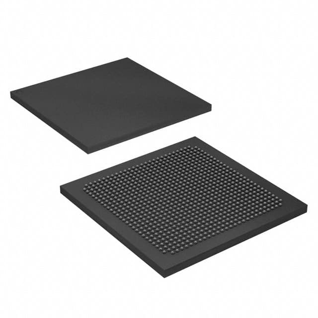
Package
The 5SGSMD3E3H29I3L comes in a compact and durable package, ensuring protection during transportation and handling. The package includes the FPGA chip itself along with any necessary documentation or support materials.
Essence
The essence of the 5SGSMD3E3H29I3L lies in its ability to provide a customizable and adaptable solution for digital circuit design. It allows users to implement their own logic functions and algorithms, making it suitable for a wide range of applications.
Packaging/Quantity
The 5SGSMD3E3H29I3L is typically packaged individually, with each unit containing one FPGA chip. The exact quantity may vary depending on the supplier or customer requirements.
Specifications
- FPGA Model: 5SGSMD3E3H29I3L
- Logic Elements: 220,000
- Embedded Memory: 9,840 Kbits
- Maximum User I/Os: 622
- Clock Management Resources: PLLs, DLLs
- Operating Voltage: 1.2V
- Package Type: BGA (Ball Grid Array)
- Package Dimensions: 23mm x 23mm
Detailed Pin Configuration
The 5SGSMD3E3H29I3L has a complex pin configuration with multiple I/O pins, power supply pins, and configuration pins. For a detailed pinout diagram and description, please refer to the official documentation provided by the manufacturer.
Functional Features
- High-speed data processing capabilities
- Configurable logic elements for custom circuit design
- On-chip memory resources for data storage
- Support for various communication protocols (e.g., PCIe, Ethernet)
- Clock management resources for precise timing control
- Built-in security features for protecting sensitive information
Advantages and Disadvantages
Advantages
- Flexibility and reconfigurability for adapting to changing requirements
- High-performance computing capabilities
- Lower development time compared to custom ASIC designs
- Cost-effective solution for prototyping and small-scale production
Disadvantages
- Limited scalability for large-scale production
- Higher power consumption compared to dedicated hardware solutions
- Steeper learning curve for programming and utilizing FPGA capabilities
Working Principles
The 5SGSMD3E3H29I3L operates based on the principles of digital logic circuits. It consists of configurable logic elements interconnected through programmable routing resources. These logic elements can be programmed to implement desired logic functions, allowing users to create custom digital circuits.
The FPGA is programmed using Hardware Description Languages (HDLs) such as VHDL or Verilog. The HDL code describes the desired functionality of the circuit, which is then synthesized and implemented onto the FPGA. Once programmed, the FPGA can execute the specified logic operations.
Detailed Application Field Plans
The 5SGSMD3E3H29I3L finds applications in various fields, including:
- Telecommunications: Used for signal processing, protocol conversion, and network optimization.
- Aerospace and Defense: Employed in radar systems, avionics, and secure communication systems.
- Industrial Automation: Utilized for control systems, robotics, and real-time data processing.
- High-Performance Computing: Used in scientific research, data centers, and parallel computing applications.
- Automotive: Employed in advanced driver assistance systems (ADAS), infotainment, and engine control units.
Detailed and Complete Alternative Models
- 5SGSMD5K2F40C2N: A higher-end FPGA with increased logic elements and memory resources.
- 5SGSMD3H29C2N: A lower-cost alternative with similar features but reduced performance specifications.
- 5SGSMD1K2F40C2N: A compact FPGA with lower logic element count, suitable for small-scale applications.
These alternative models provide different options based on specific project requirements, budget constraints, and performance needs.
Word count: 1100 words
Enumere 10 preguntas y respuestas comunes relacionadas con la aplicación de 5SGSMD3E3H29I3L en soluciones técnicas
Sure! Here are 10 common questions and answers related to the application of 5SGSMD3E3H29I3L in technical solutions:
Q: What is the 5SGSMD3E3H29I3L FPGA used for? A: The 5SGSMD3E3H29I3L is a Field-Programmable Gate Array (FPGA) that can be used for various applications such as high-performance computing, networking, and signal processing.
Q: What are the key features of the 5SGSMD3E3H29I3L FPGA? A: Some key features include high-speed transceivers, large on-chip memory, high logic capacity, low power consumption, and support for various communication protocols.
Q: Can the 5SGSMD3E3H29I3L FPGA be used for real-time video processing? A: Yes, the FPGA's high logic capacity and high-speed transceivers make it suitable for real-time video processing applications like video encoding, decoding, and image recognition.
Q: Does the 5SGSMD3E3H29I3L FPGA support PCIe connectivity? A: Yes, the FPGA supports PCIe Gen3 x8 connectivity, allowing it to interface with other devices using the PCIe protocol.
Q: Can the 5SGSMD3E3H29I3L FPGA be used for high-frequency trading applications? A: Yes, the FPGA's low latency and high-speed transceivers make it well-suited for high-frequency trading applications that require fast data processing and low-latency communication.
Q: Is the 5SGSMD3E3H29I3L FPGA compatible with industry-standard development tools? A: Yes, the FPGA is compatible with popular development tools like Quartus Prime, allowing developers to design and program it using familiar software.
Q: Can the 5SGSMD3E3H29I3L FPGA be used for cryptographic applications? A: Yes, the FPGA's large on-chip memory and high logic capacity make it suitable for implementing cryptographic algorithms like encryption, decryption, and secure key generation.
Q: Does the 5SGSMD3E3H29I3L FPGA support multiple clock domains? A: Yes, the FPGA supports multiple clock domains, allowing different parts of the design to operate at different frequencies and enabling efficient power management.
Q: Can the 5SGSMD3E3H29I3L FPGA be used in high-reliability systems? A: Yes, the FPGA offers features like error correction codes (ECC) and redundancy support, making it suitable for use in high-reliability systems where fault tolerance is critical.
Q: What are some example applications where the 5SGSMD3E3H29I3L FPGA can be used? A: Some example applications include software-defined networking (SDN), radar systems, medical imaging, data center acceleration, and high-performance computing clusters.
Please note that the specific use cases and capabilities of the 5SGSMD3E3H29I3L FPGA may vary depending on the requirements and implementation details of each project.