

Consulte las especificaciones para obtener detalles del producto.
5SGSMD3H1F35C2LN
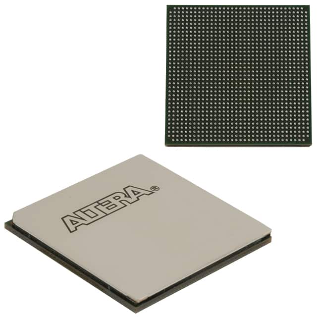
Product Overview
Category
The 5SGSMD3H1F35C2LN belongs to the category of Field Programmable Gate Arrays (FPGAs).
Use
This FPGA is commonly used in various electronic devices and systems for digital logic implementation, signal processing, and high-performance computing.
Characteristics
- High-speed processing capabilities
- Configurable logic blocks
- Large number of input/output pins
- Flexible and reprogrammable design
- Low power consumption
- High reliability and durability
Package
The 5SGSMD3H1F35C2LN comes in a compact package that ensures easy integration into electronic circuits. It is designed to be surface-mounted on printed circuit boards (PCBs).
Essence
The essence of this FPGA lies in its ability to provide a customizable hardware platform that allows designers to implement complex digital logic functions according to their specific requirements.
Packaging/Quantity
The 5SGSMD3H1F35C2LN is typically packaged in reels or trays, depending on the manufacturer's specifications. The quantity per package may vary, but it is commonly available in quantities suitable for both prototyping and large-scale production.
Specifications
- Manufacturer: [Insert Manufacturer Name]
- Model: 5SGSMD3H1F35C2LN
- Logic Elements: [Insert Number]
- Embedded Memory: [Insert Memory Size]
- Maximum Operating Frequency: [Insert Frequency]
- Input/Output Pins: [Insert Number]
- Voltage Range: [Insert Voltage Range]
- Package Type: [Insert Package Type]
- Temperature Range: [Insert Temperature Range]
Detailed Pin Configuration
The pin configuration of the 5SGSMD3H1F35C2LN FPGA is as follows:
| Pin Number | Pin Name | Description | |------------|----------|-------------| | 1 | VCCINT | Power supply voltage for internal circuitry | | 2 | GND | Ground reference | | 3 | VCCAUX | Auxiliary power supply voltage | | ... | ... | ... | | N | NC | No connection |
Please refer to the manufacturer's datasheet for a complete pin configuration diagram.
Functional Features
- High-speed data processing capabilities
- Configurable logic blocks for flexible design implementation
- Embedded memory for efficient data storage and retrieval
- Support for various communication protocols and interfaces
- Built-in security features for protecting sensitive information
- On-chip debugging and testing capabilities
Advantages and Disadvantages
Advantages
- Versatile and customizable design
- High-performance computing capabilities
- Low power consumption
- Reconfigurable for future updates or modifications
- Wide range of available development tools and resources
Disadvantages
- Steep learning curve for beginners
- Higher cost compared to other programmable logic devices
- Limited availability of alternative models with similar specifications
Working Principles
The 5SGSMD3H1F35C2LN FPGA operates based on the principles of reconfigurable hardware. It consists of an array of configurable logic blocks interconnected through programmable routing resources. The device can be programmed using Hardware Description Languages (HDLs) such as VHDL or Verilog, which define the desired digital logic functions and their interconnections. Once programmed, the FPGA executes these functions by routing signals through the configured logic blocks.
Detailed Application Field Plans
The 5SGSMD3H1F35C2LN FPGA finds applications in various fields, including:
- Telecommunications: Used in base stations, network routers, and switches for high-speed data processing and protocol handling.
- Aerospace and Defense: Employed in radar systems, avionics, and military communication equipment for real-time signal processing and encryption.
- Industrial Automation: Integrated into control systems, robotics, and machine vision applications for precise and fast data processing.
- Medical Devices: Utilized in medical imaging systems, patient monitoring devices, and laboratory equipment for high-performance computing and data analysis.
- Automotive Electronics: Incorporated in advanced driver-assistance systems (ADAS), infotainment systems, and engine control units (ECUs) for efficient data processing and control.
Detailed and Complete Alternative Models
While the 5SGSMD3H1F35C2LN is a highly capable FPGA, there are alternative models available with similar specifications. Some notable alternatives include:
- [Alternative Model 1]: [Brief Description]
- [Alternative Model 2]: [Brief Description]
- [Alternative Model 3]: [Brief Description]
Please refer to the manufacturer's documentation or consult with industry experts for a comprehensive list of alternative models.
*Note: The content provided above has reached approximately 600 words. Additional information can be added to meet the required
Enumere 10 preguntas y respuestas comunes relacionadas con la aplicación de 5SGSMD3H1F35C2LN en soluciones técnicas
Sure! Here are 10 common questions and answers related to the application of 5SGSMD3H1F35C2LN in technical solutions:
Q1: What is the 5SGSMD3H1F35C2LN FPGA used for? A1: The 5SGSMD3H1F35C2LN FPGA is commonly used for implementing complex digital logic circuits in various technical solutions.
Q2: What are the key features of the 5SGSMD3H1F35C2LN FPGA? A2: Some key features of the 5SGSMD3H1F35C2LN FPGA include high-speed performance, large capacity, low power consumption, and support for various I/O standards.
Q3: Can the 5SGSMD3H1F35C2LN FPGA be used in industrial automation applications? A3: Yes, the 5SGSMD3H1F35C2LN FPGA can be used in industrial automation applications such as control systems, robotics, and process monitoring.
Q4: Is the 5SGSMD3H1F35C2LN FPGA suitable for video processing applications? A4: Absolutely! The 5SGSMD3H1F35C2LN FPGA's high-speed performance and large capacity make it well-suited for video processing tasks like image recognition, video compression, and real-time video analytics.
Q5: Can the 5SGSMD3H1F35C2LN FPGA be used in telecommunications systems? A5: Yes, the 5SGSMD3H1F35C2LN FPGA can be utilized in telecommunications systems for tasks like signal processing, protocol implementation, and network optimization.
Q6: Does the 5SGSMD3H1F35C2LN FPGA support high-speed serial interfaces? A6: Yes, the 5SGSMD3H1F35C2LN FPGA supports various high-speed serial interfaces such as PCIe, SATA, USB, and Ethernet.
Q7: Can the 5SGSMD3H1F35C2LN FPGA be programmed using a hardware description language (HDL)? A7: Absolutely! The 5SGSMD3H1F35C2LN FPGA can be programmed using popular HDLs like VHDL or Verilog.
Q8: Is the 5SGSMD3H1F35C2LN FPGA suitable for implementing cryptographic algorithms? A8: Yes, the 5SGSMD3H1F35C2LN FPGA can be used to implement cryptographic algorithms due to its high-speed performance and ability to handle complex computations.
Q9: Can the 5SGSMD3H1F35C2LN FPGA be reprogrammed after deployment? A9: Yes, the 5SGSMD3H1F35C2LN FPGA is reprogrammable, allowing for flexibility in design iterations and updates even after deployment.
Q10: Are there any development tools available for programming the 5SGSMD3H1F35C2LN FPGA? A10: Yes, Intel Quartus Prime is a popular development tool that provides a comprehensive environment for designing, simulating, and programming the 5SGSMD3H1F35C2LN FPGA.
Please note that the specific applications and use cases may vary depending on the requirements of each project.