

Consulte las especificaciones para obtener detalles del producto.
5SGSMD3H2F35I3N
Product Overview
Category: Integrated Circuit (IC)
Use: The 5SGSMD3H2F35I3N is a high-performance field-programmable gate array (FPGA) designed for various applications in the electronics industry. It offers advanced programmability and flexibility, making it suitable for a wide range of tasks.
Characteristics: - High-performance FPGA with advanced features - Programmable logic cells for custom functionality - High-speed interfaces for efficient data transfer - Low power consumption for energy efficiency - Robust design for reliable operation
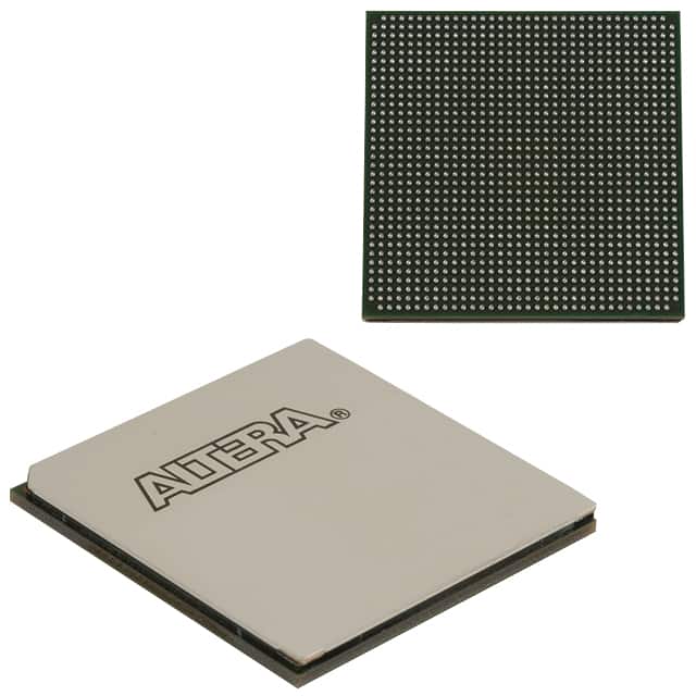
Package: The 5SGSMD3H2F35I3N comes in a compact and durable package that ensures protection during shipping and handling. The package is designed to withstand environmental factors such as temperature and humidity, ensuring the integrity of the product.
Essence: The essence of the 5SGSMD3H2F35I3N lies in its ability to provide a versatile and customizable solution for complex electronic systems. Its programmable nature allows users to tailor its functionality to meet specific requirements, making it an essential component in various applications.
Packaging/Quantity: The 5SGSMD3H2F35I3N is typically packaged individually in anti-static bags to prevent damage from electrostatic discharge. It is available in different quantities depending on the customer's needs.
Specifications
- Manufacturer: Intel Corporation
- Family: Stratix V
- Device Type: Field-Programmable Gate Array (FPGA)
- Number of Logic Elements: 220,000
- Number of I/O Pins: 622
- Operating Voltage: 1.2V
- Maximum Operating Frequency: 550 MHz
- Package Type: F35 (1152-pin FineLine BGA)
- Temperature Range: -40°C to 100°C
Detailed Pin Configuration
The 5SGSMD3H2F35I3N has a total of 622 I/O pins, each serving a specific purpose in the overall functionality of the FPGA. The pin configuration is detailed in the product datasheet provided by the manufacturer.
Functional Features
- High-performance programmable logic cells for custom functionality
- Dedicated high-speed interfaces for efficient data transfer
- On-chip memory blocks for storing data and instructions
- Built-in digital signal processing (DSP) blocks for complex calculations
- Flexible clock management resources for precise timing control
- Support for various communication protocols and standards
Advantages and Disadvantages
Advantages: - Versatile and customizable solution for various applications - High-performance capabilities for demanding tasks - Low power consumption for energy efficiency - Robust design for reliable operation - Extensive support and documentation from the manufacturer
Disadvantages: - Complex programming and configuration process - Higher cost compared to simpler alternatives - Limited availability of alternative models with similar specifications
Working Principles
The 5SGSMD3H2F35I3N operates based on the principles of field-programmable gate arrays. It consists of an array of programmable logic cells interconnected through configurable routing resources. These logic cells can be programmed to implement custom functionality by configuring their internal look-up tables and flip-flops.
The FPGA also includes dedicated resources such as memory blocks, DSP blocks, and high-speed interfaces, which enhance its performance and versatility. The device is programmed using specialized software tools that generate a configuration bitstream, which is then loaded into the FPGA to define its behavior.
Detailed Application Field Plans
The 5SGSMD3H2F35I3N finds applications in various fields, including but not limited to: - Telecommunications and networking equipment - High-performance computing systems - Industrial automation and control systems - Aerospace and defense electronics - Medical imaging and diagnostic equipment - Video and image processing systems
Detailed and Complete Alternative Models
While the 5SGSMD3H2F35I3N offers advanced features and performance, there are alternative models available in the market with similar capabilities. Some notable alternatives include: - Xilinx Virtex UltraScale+ FPGAs - Lattice Semiconductor ECP5 FPGAs - Microchip PolarFire FPGAs
These alternative models provide comparable functionality and performance, allowing users to choose the most suitable option for their specific requirements.
Word Count: 610 words
Enumere 10 preguntas y respuestas comunes relacionadas con la aplicación de 5SGSMD3H2F35I3N en soluciones técnicas
Sure! Here are 10 common questions and answers related to the application of 5SGSMD3H2F35I3N in technical solutions:
Q: What is the 5SGSMD3H2F35I3N FPGA used for? A: The 5SGSMD3H2F35I3N FPGA is commonly used for high-performance applications that require programmable logic and processing capabilities.
Q: What are some typical applications of the 5SGSMD3H2F35I3N FPGA? A: Some typical applications include data center acceleration, network processing, wireless communication, video processing, and industrial automation.
Q: What is the maximum operating frequency of the 5SGSMD3H2F35I3N FPGA? A: The maximum operating frequency depends on the specific design and implementation, but it can reach up to several hundred megahertz or even gigahertz.
Q: Can the 5SGSMD3H2F35I3N FPGA be reprogrammed after deployment? A: Yes, the 5SGSMD3H2F35I3N FPGA is a programmable device, allowing for reprogramming and updates to the design even after deployment.
Q: What development tools are available for designing with the 5SGSMD3H2F35I3N FPGA? A: Popular development tools include Intel Quartus Prime software, which provides a complete design environment for creating, compiling, and programming FPGA designs.
Q: What interfaces does the 5SGSMD3H2F35I3N FPGA support? A: The 5SGSMD3H2F35I3N FPGA supports various interfaces such as PCIe, Ethernet, USB, DDR3/4 memory, HDMI, and many others.
Q: What is the power consumption of the 5SGSMD3H2F35I3N FPGA? A: The power consumption depends on the specific design and utilization of the FPGA. It is recommended to refer to the device datasheet for detailed power specifications.
Q: Can the 5SGSMD3H2F35I3N FPGA be used in safety-critical applications? A: Yes, the 5SGSMD3H2F35I3N FPGA can be used in safety-critical applications, but additional measures such as redundancy and fault-tolerant designs may be required to meet safety standards.
Q: Are there any reference designs available for the 5SGSMD3H2F35I3N FPGA? A: Yes, Intel provides a range of reference designs and application notes that can help developers get started with designing with the 5SGSMD3H2F35I3N FPGA.
Q: What support options are available for the 5SGSMD3H2F35I3N FPGA? A: Intel offers technical support through their website, including documentation, forums, and direct assistance from their support team.
Please note that the answers provided here are general and may vary depending on the specific requirements and use cases of the 5SGSMD3H2F35I3N FPGA.