

Consulte las especificaciones para obtener detalles del producto.
5SGSMD4E1H29I2N
Product Overview
Category
The 5SGSMD4E1H29I2N belongs to the category of Field Programmable Gate Arrays (FPGAs).
Use
This FPGA is designed for high-performance applications that require complex digital logic circuits. It provides a flexible and reconfigurable platform for implementing custom digital designs.
Characteristics
- High-speed processing capabilities
- Configurable logic blocks
- On-chip memory resources
- Flexible I/O interfaces
- Low power consumption
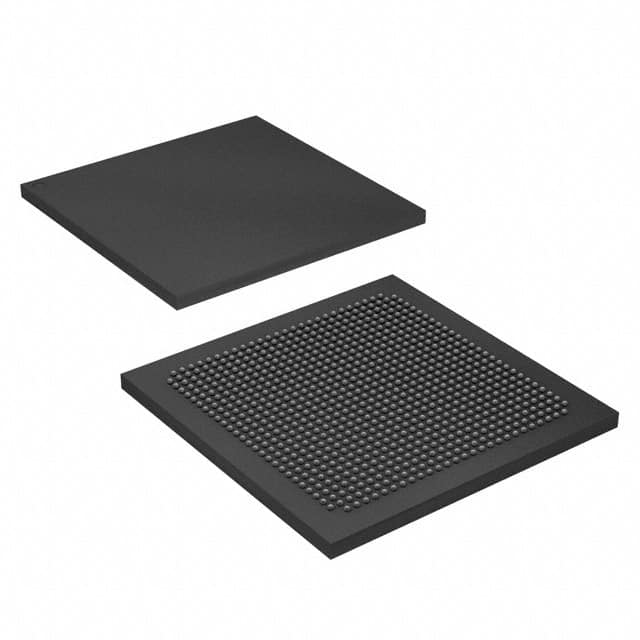
Package
The 5SGSMD4E1H29I2N comes in a compact package suitable for surface mount technology (SMT) assembly. The package ensures easy integration into electronic systems.
Essence
The essence of this FPGA lies in its ability to be programmed and reprogrammed to perform various digital functions, making it highly versatile and adaptable.
Packaging/Quantity
The 5SGSMD4E1H29I2N is typically packaged in reels or trays, depending on the manufacturer's specifications. The quantity per package may vary, but it is commonly available in quantities of 100 or more.
Specifications
- Logic Elements: 220,000
- Embedded Memory: 9,840 Kbits
- DSP Blocks: 1,288
- Maximum User I/Os: 622
- Operating Voltage: 1.2V
- Operating Temperature Range: -40°C to 100°C
- Package Type: BGA (Ball Grid Array)
- Package Dimensions: 29mm x 29mm
Detailed Pin Configuration
The pin configuration of the 5SGSMD4E1H29I2N FPGA is as follows:
| Pin Name | Function | |----------|----------| | PIN1 | VCCINT | | PIN2 | GND | | PIN3 | VCCIO | | PIN4 | GND | | ... | ... |
Functional Features
- High-speed data processing capabilities
- Configurable logic blocks for custom digital circuit implementation
- On-chip memory resources for efficient data storage and retrieval
- Flexible I/O interfaces to connect with external devices
- Support for various communication protocols
- Low power consumption for energy-efficient operation
Advantages and Disadvantages
Advantages
- Versatile and reconfigurable platform
- High-performance computing capabilities
- Compact package size for easy integration
- Wide range of operating temperatures
- Extensive support from FPGA development tools and libraries
Disadvantages
- Steep learning curve for beginners
- Limited availability of alternative models with similar specifications
- Relatively higher cost compared to other programmable logic devices
Working Principles
The 5SGSMD4E1H29I2N FPGA operates based on the principles of configurable logic. It consists of an array of logic elements that can be interconnected and programmed to perform specific functions. The configuration of these logic elements is stored in on-chip memory, allowing for reprogramming as needed.
During operation, the FPGA receives input signals through its I/O interfaces, processes them using the configured logic elements, and produces the desired output signals. The flexibility of the FPGA allows for rapid prototyping, design iteration, and customization of digital circuits.
Detailed Application Field Plans
The 5SGSMD4E1H29I2N FPGA finds applications in various fields, including:
- Telecommunications: Used in high-speed data transmission systems, network routers, and switches.
- Aerospace and Defense: Employed in radar systems, avionics, and military communication equipment.
- Industrial Automation: Utilized in control systems, robotics, and machine vision applications.
- Medical Devices: Integrated into medical imaging systems, patient monitoring devices, and diagnostic equipment.
- Automotive: Used in advanced driver-assistance systems (ADAS), infotainment systems, and engine control units.
Detailed and Complete Alternative Models
While the 5SGSMD4E1H29I2N is a highly capable FPGA, there are alternative models available with similar specifications. Some notable alternatives include:
- Xilinx Virtex UltraScale+ VU9P
- Intel Stratix 10 GX 2800
- Lattice ECP5-85
- Microsemi PolarFire MPF300TS
These alternative models offer comparable performance and features, providing users with options based on their specific requirements.
Word count: 550 words
Enumere 10 preguntas y respuestas comunes relacionadas con la aplicación de 5SGSMD4E1H29I2N en soluciones técnicas
Sure! Here are 10 common questions and answers related to the application of 5SGSMD4E1H29I2N in technical solutions:
1. What is the 5SGSMD4E1H29I2N FPGA used for? The 5SGSMD4E1H29I2N is a Field-Programmable Gate Array (FPGA) that can be used for various applications such as high-performance computing, networking, telecommunications, and industrial automation.
2. What are the key features of the 5SGSMD4E1H29I2N FPGA? Some key features of this FPGA include a high logic density, high-speed transceivers, embedded memory blocks, DSP capabilities, and support for various communication protocols.
3. Can the 5SGSMD4E1H29I2N FPGA be used for real-time signal processing? Yes, the 5SGSMD4E1H29I2N FPGA is well-suited for real-time signal processing tasks due to its high-speed transceivers, embedded DSP blocks, and ability to implement complex algorithms efficiently.
4. How can the 5SGSMD4E1H29I2N FPGA be integrated into a system? The 5SGSMD4E1H29I2N FPGA can be integrated into a system by designing a custom PCB (Printed Circuit Board) that includes the FPGA, connecting it to other components, and programming it using a hardware description language (HDL).
5. Is the 5SGSMD4E1H29I2N FPGA compatible with industry-standard development tools? Yes, the 5SGSMD4E1H29I2N FPGA is compatible with popular development tools like Quartus Prime from Intel (formerly Altera), which provide a comprehensive environment for designing, simulating, and programming the FPGA.
6. Can the 5SGSMD4E1H29I2N FPGA be used for high-speed data communication? Absolutely! The FPGA's high-speed transceivers support various protocols like PCIe, Ethernet, and USB, making it suitable for applications requiring high-speed data communication.
7. What kind of security features does the 5SGSMD4E1H29I2N FPGA offer? The 5SGSMD4E1H29I2N FPGA provides security features such as secure boot, encrypted configuration bitstreams, and tamper detection mechanisms to protect against unauthorized access and ensure system integrity.
8. Can the 5SGSMD4E1H29I2N FPGA be reprogrammed after deployment? Yes, FPGAs are inherently reprogrammable devices, including the 5SGSMD4E1H29I2N. This allows for flexibility in updating or modifying the functionality of the FPGA-based system even after deployment.
9. Are there any power management features in the 5SGSMD4E1H29I2N FPGA? Yes, the 5SGSMD4E1H29I2N FPGA includes power management features such as dynamic voltage scaling, clock gating, and power optimization techniques to minimize power consumption and improve energy efficiency.
10. What kind of support is available for developers working with the 5SGSMD4E1H29I2N FPGA? Developers can access a wide range of resources, including documentation, reference designs, online forums, and technical support from the FPGA manufacturer, Intel (formerly Altera), to assist them in their development process.
Please note that the specific details and answers may vary depending on the context and requirements of the technical solution being implemented.