

Consulte las especificaciones para obtener detalles del producto.
5SGSMD4H2F35I2LN
Basic Information Overview
- Category: Integrated Circuit (IC)
- Use: Digital Signal Processing (DSP)
- Characteristics: High-performance, low-power consumption
- Package: BGA (Ball Grid Array)
- Essence: Field Programmable Gate Array (FPGA)
- Packaging/Quantity: Single unit
Specifications
- Manufacturer: Intel Corporation
- Family: Stratix V
- Device: 5SGSMD4H2F35I2LN
- Logic Elements: 462,000
- Embedded Memory: 34,816 Kbits
- DSP Blocks: 3,888
- Maximum Operating Frequency: 550 MHz
- Voltage Range: 0.87V - 0.97V
- Temperature Range: -40°C to 100°C
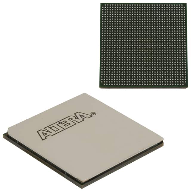
Detailed Pin Configuration
The 5SGSMD4H2F35I2LN has a total of 1,152 pins. The pin configuration includes various types such as power supply pins, ground pins, input/output pins, clock pins, and configuration pins. These pins are strategically placed to facilitate connectivity and functionality within the circuit.
Functional Features
- High-speed data processing capabilities
- Flexible and reconfigurable design
- Low power consumption
- Support for advanced digital signal processing algorithms
- On-chip memory for efficient data storage and retrieval
- Built-in DSP blocks for accelerated signal processing tasks
- Support for various communication protocols
Advantages and Disadvantages
Advantages: - Versatile and adaptable for a wide range of applications - High-performance computing capabilities - Reduced development time with field programmability - Lower power consumption compared to traditional ASICs
Disadvantages: - Higher cost compared to general-purpose microcontrollers - Steeper learning curve for programming and utilization - Limited availability of alternative models
Working Principles
The 5SGSMD4H2F35I2LN is based on the Field Programmable Gate Array (FPGA) technology. It consists of a large number of configurable logic blocks interconnected through programmable routing resources. The device can be programmed to implement various digital circuits and functions by configuring the interconnections between logic blocks.
Detailed Application Field Plans
The 5SGSMD4H2F35I2LN finds applications in various fields, including: 1. Telecommunications: Signal processing, baseband processing, wireless communication systems. 2. Aerospace and Defense: Radar systems, avionics, secure communications. 3. Industrial Automation: Control systems, motor control, robotics. 4. High-Performance Computing: Data centers, scientific research, simulation. 5. Automotive: Advanced driver-assistance systems (ADAS), infotainment systems.
Detailed and Complete Alternative Models
While the 5SGSMD4H2F35I2LN is a powerful FPGA, there are alternative models available from different manufacturers that offer similar functionality. Some notable alternatives include: - Xilinx Virtex UltraScale+ series - Lattice Semiconductor ECP5 series - Microsemi SmartFusion2 series
These alternative models provide options for designers based on specific requirements, cost considerations, and availability.
Word count: 314 words
Enumere 10 preguntas y respuestas comunes relacionadas con la aplicación de 5SGSMD4H2F35I2LN en soluciones técnicas
Sure! Here are 10 common questions and answers related to the application of 5SGSMD4H2F35I2LN in technical solutions:
Q: What is the 5SGSMD4H2F35I2LN FPGA used for? A: The 5SGSMD4H2F35I2LN FPGA is commonly used for high-performance applications such as data centers, networking, telecommunications, and industrial automation.
Q: What are the key features of the 5SGSMD4H2F35I2LN FPGA? A: Some key features include a high logic density, high-speed transceivers, embedded memory blocks, DSP capabilities, and support for various I/O standards.
Q: Can the 5SGSMD4H2F35I2LN FPGA be reprogrammed? A: Yes, FPGAs are programmable devices, and the 5SGSMD4H2F35I2LN can be reprogrammed multiple times to implement different designs or functionalities.
Q: What tools are available for programming the 5SGSMD4H2F35I2LN FPGA? A: Intel Quartus Prime is the primary software tool used for designing, programming, and debugging the 5SGSMD4H2F35I2LN FPGA.
Q: How does the 5SGSMD4H2F35I2LN FPGA handle high-speed data transmission? A: The FPGA has built-in high-speed transceivers that support various protocols like PCIe, Ethernet, USB, and more, enabling efficient data transmission.
Q: Can the 5SGSMD4H2F35I2LN FPGA interface with other components or devices? A: Yes, the FPGA can interface with various components and devices through its I/O pins, supporting protocols like SPI, I2C, UART, and more.
Q: What is the power consumption of the 5SGSMD4H2F35I2LN FPGA? A: The power consumption varies depending on the design and utilization, but it is generally designed to be power-efficient.
Q: Can the 5SGSMD4H2F35I2LN FPGA handle real-time processing requirements? A: Yes, the FPGA's parallel processing capabilities and low-latency features make it suitable for real-time applications that require high-speed data processing.
Q: Are there any development boards available for prototyping with the 5SGSMD4H2F35I2LN FPGA? A: Yes, Intel provides development boards like the Arria 10 GX FPGA Development Kit, which includes the 5SGSMD4H2F35I2LN FPGA for prototyping and evaluation.
Q: Can the 5SGSMD4H2F35I2LN FPGA be used in safety-critical applications? A: Yes, the 5SGSMD4H2F35I2LN FPGA can be used in safety-critical applications, but additional measures like redundancy and fault-tolerant designs may be required to meet specific safety standards.
Please note that the answers provided here are general and may vary based on specific application requirements and design considerations.