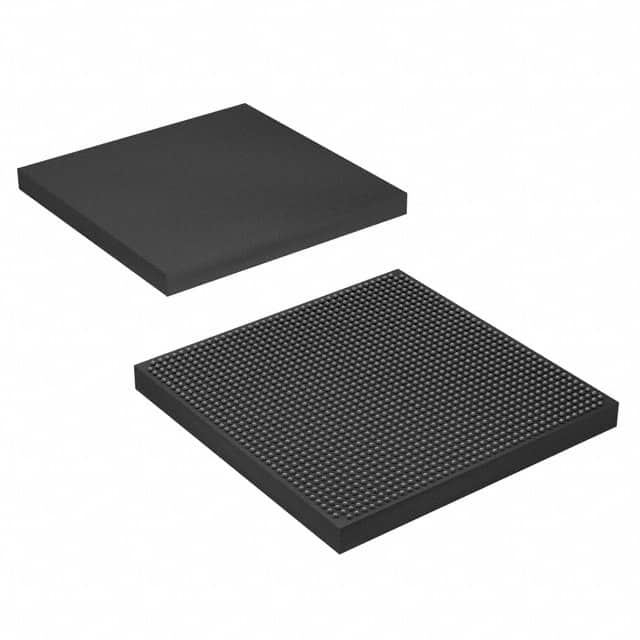
Consulte las especificaciones para obtener detalles del producto.

5SGSMD5K3F40I4
Basic Information Overview
- Category: Integrated Circuit (IC)
- Use: Digital Signal Processing (DSP)
- Characteristics: High-performance, low-power consumption
- Package: BGA (Ball Grid Array)
- Essence: Field Programmable Gate Array (FPGA)
- Packaging/Quantity: Single unit
Specifications
- Manufacturer: Intel Corporation
- Family: Stratix V
- Device: 5SGSMD5K3F40I4
- Logic Elements: 462,000
- Embedded Memory: 34,560 Kbits
- DSP Blocks: 2,530
- Maximum Operating Frequency: 400 MHz
- Operating Voltage: 1.0V
- Temperature Range: -40°C to +100°C
Detailed Pin Configuration
The 5SGSMD5K3F40I4 has a complex pin configuration with a total of 1,040 pins. The pins are distributed across different functional groups such as power supply, clock inputs, general-purpose I/Os, memory interfaces, and high-speed transceivers.
For a detailed pin configuration diagram, please refer to the official datasheet provided by the manufacturer.
Functional Features
- High-performance processing capabilities for digital signal processing applications.
- Low-power consumption design for energy-efficient operation.
- Flexible and reconfigurable architecture allows for customization and adaptation to various tasks.
- Advanced memory interfaces enable efficient data storage and retrieval.
- High-speed transceivers facilitate fast communication with external devices.
Advantages and Disadvantages
Advantages: - Versatile and adaptable for a wide range of applications. - High-performance processing capabilities. - Low-power consumption design. - Efficient memory interfaces and high-speed transceivers.
Disadvantages: - Complex pin configuration may require careful planning and layout considerations. - Limited availability of alternative models with similar specifications.
Working Principles
The 5SGSMD5K3F40I4 is based on the Field Programmable Gate Array (FPGA) technology. It consists of a large number of configurable logic blocks, memory elements, and programmable interconnects. The device can be programmed to implement various digital circuits and functions by configuring the interconnections and functionality of its internal components.
During operation, the FPGA is configured with a specific design using a hardware description language or a graphical programming tool. The configuration data is stored in non-volatile memory within the device. Once configured, the FPGA performs the desired functions by routing signals through the programmable interconnects and executing the programmed logic within the configurable logic blocks.
Detailed Application Field Plans
The 5SGSMD5K3F40I4 finds applications in various fields that require high-performance digital signal processing capabilities. Some of the common application areas include: - Telecommunications: Signal processing for wireless communication systems, baseband processing, and protocol implementation. - Video and Image Processing: Real-time video processing, image recognition, and computer vision applications. - Industrial Automation: Control systems, motor control, and real-time monitoring. - Aerospace and Defense: Radar and sonar signal processing, encryption/decryption, and secure communications. - High-Performance Computing: Acceleration of complex algorithms, scientific simulations, and data analytics.
Detailed and Complete Alternative Models
While the 5SGSMD5K3F40I4 offers a unique combination of features and specifications, there are alternative FPGA models available from different manufacturers that may suit specific requirements. Some alternative models to consider are: - Xilinx Virtex UltraScale+ series - Lattice Semiconductor ECP5 series - Microsemi SmartFusion2 series
These alternative models offer varying performance levels, power consumption, and package options. It is recommended to consult the respective manufacturers' documentation for detailed specifications and compatibility with specific application requirements.
Word count: 455 words
Enumere 10 preguntas y respuestas comunes relacionadas con la aplicación de 5SGSMD5K3F40I4 en soluciones técnicas
Sure! Here are 10 common questions and answers related to the application of 5SGSMD5K3F40I4 in technical solutions:
Q: What is the 5SGSMD5K3F40I4 FPGA used for? A: The 5SGSMD5K3F40I4 FPGA is commonly used for high-performance applications that require programmable logic, such as data centers, networking equipment, and industrial automation.
Q: What are the key features of the 5SGSMD5K3F40I4 FPGA? A: Some key features of the 5SGSMD5K3F40I4 FPGA include a high logic density, high-speed transceivers, embedded memory blocks, and support for various I/O standards.
Q: Can the 5SGSMD5K3F40I4 FPGA be reprogrammed? A: Yes, the 5SGSMD5K3F40I4 FPGA is reprogrammable, allowing users to modify the functionality of the device even after it has been deployed.
Q: What programming languages can be used with the 5SGSMD5K3F40I4 FPGA? A: The 5SGSMD5K3F40I4 FPGA can be programmed using hardware description languages (HDLs) such as Verilog or VHDL.
Q: How does the 5SGSMD5K3F40I4 FPGA handle high-speed data transmission? A: The 5SGSMD5K3F40I4 FPGA includes high-speed transceivers that support various protocols like PCIe, Ethernet, and USB, enabling efficient data transmission.
Q: Can the 5SGSMD5K3F40I4 FPGA interface with other components or devices? A: Yes, the 5SGSMD5K3F40I4 FPGA can interface with other components or devices through its I/O pins, allowing for seamless integration into larger systems.
Q: What kind of memory resources does the 5SGSMD5K3F40I4 FPGA offer? A: The 5SGSMD5K3F40I4 FPGA provides embedded memory blocks (RAM) that can be used for storing data or implementing complex algorithms.
Q: Can the 5SGSMD5K3F40I4 FPGA handle real-time processing requirements? A: Yes, the 5SGSMD5K3F40I4 FPGA is capable of handling real-time processing tasks due to its high logic density and parallel processing capabilities.
Q: Are there any development tools available for programming the 5SGSMD5K3F40I4 FPGA? A: Yes, Intel Quartus Prime is a popular development tool that supports programming and debugging of the 5SGSMD5K3F40I4 FPGA.
Q: Can the 5SGSMD5K3F40I4 FPGA be used in safety-critical applications? A: Yes, the 5SGSMD5K3F40I4 FPGA can be used in safety-critical applications, but additional measures may be required to ensure functional safety compliance.
Please note that the specific details and answers may vary depending on the context and application requirements.

