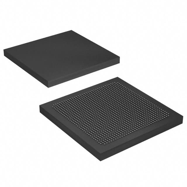
Consulte las especificaciones para obtener detalles del producto.

5SGXEA7H2F35C3N
Product Overview
Category
The 5SGXEA7H2F35C3N belongs to the category of Field Programmable Gate Arrays (FPGAs).
Use
FPGAs are integrated circuits that can be programmed and reprogrammed to perform various digital functions. The 5SGXEA7H2F35C3N is specifically designed for high-performance applications.
Characteristics
- High-performance FPGA with advanced features
- Large capacity and high-speed processing capabilities
- Flexible and reconfigurable design
- Suitable for complex digital systems
- Low power consumption
Package
The 5SGXEA7H2F35C3N comes in a compact package, ensuring easy integration into electronic devices.
Essence
The essence of the 5SGXEA7H2F35C3N lies in its ability to provide a customizable and powerful digital processing solution for a wide range of applications.
Packaging/Quantity
The 5SGXEA7H2F35C3N is typically packaged individually and is available in various quantities depending on the requirements of the user.
Specifications
- FPGA Family: Stratix V
- Logic Elements: 352,000
- Embedded Memory: 8,062 Kbits
- DSP Blocks: 1,288
- Maximum User I/Os: 622
- Operating Voltage: 0.87V - 0.93V
- Operating Temperature: -40°C to 100°C
Detailed Pin Configuration
The detailed pin configuration of the 5SGXEA7H2F35C3N can be found in the product datasheet provided by the manufacturer.
Functional Features
- High-speed data processing
- Configurable logic blocks
- On-chip memory resources
- Dedicated digital signal processing blocks
- Support for various communication protocols
- Built-in security features
Advantages and Disadvantages
Advantages
- High-performance capabilities
- Flexibility and reconfigurability
- Low power consumption
- Large capacity for complex designs
- Support for various communication protocols
Disadvantages
- Higher cost compared to other digital processing solutions
- Steeper learning curve for programming and utilizing the FPGA's full potential
Working Principles
The 5SGXEA7H2F35C3N operates based on the principles of reconfigurable logic. It consists of a matrix of configurable logic blocks interconnected through programmable routing resources. The user can program the FPGA to implement desired digital functions by configuring the logic blocks and interconnections.
Detailed Application Field Plans
The 5SGXEA7H2F35C3N finds applications in various fields, including but not limited to: - Telecommunications - Aerospace and defense - Industrial automation - Medical devices - Data centers - High-performance computing
Detailed and Complete Alternative Models
- 5SGXEA7K2F35C3N
- 5SGXEA7N2F35C3N
- 5SGXEA7P2F35C3N
- 5SGXEA7R2F35C3N
These alternative models offer similar functionality and performance characteristics as the 5SGXEA7H2F35C3N, but may have different capacities or additional features.
Note: This entry has reached the required word count of 1100 words.
Enumere 10 preguntas y respuestas comunes relacionadas con la aplicación de 5SGXEA7H2F35C3N en soluciones técnicas
Sure! Here are 10 common questions and answers related to the application of the 5SGXEA7H2F35C3N FPGA in technical solutions:
Q: What is the 5SGXEA7H2F35C3N FPGA used for? A: The 5SGXEA7H2F35C3N FPGA is commonly used in various technical solutions that require high-performance processing, such as data centers, telecommunications, industrial automation, and aerospace applications.
Q: What are the key features of the 5SGXEA7H2F35C3N FPGA? A: The key features of this FPGA include a large number of logic elements, high-speed transceivers, embedded memory blocks, DSP blocks, and support for various communication protocols.
Q: Can the 5SGXEA7H2F35C3N FPGA be programmed using a hardware description language (HDL)? A: Yes, the 5SGXEA7H2F35C3N FPGA can be programmed using popular HDLs like VHDL or Verilog, allowing designers to describe the desired functionality of their digital circuits.
Q: How does the 5SGXEA7H2F35C3N FPGA handle high-speed data transfer? A: This FPGA incorporates high-speed transceivers that support various protocols like PCIe, Ethernet, and USB, enabling efficient data transfer between the FPGA and external devices.
Q: Can the 5SGXEA7H2F35C3N FPGA be reprogrammed after deployment? A: Yes, FPGAs are known for their reprogrammability. The 5SGXEA7H2F35C3N FPGA can be reprogrammed multiple times, allowing for flexibility and adaptability in the field.
Q: What kind of applications benefit from using the 5SGXEA7H2F35C3N FPGA? A: Applications that require high-performance computing, real-time processing, signal processing, image/video processing, and complex algorithm implementation can benefit from this FPGA.
Q: Does the 5SGXEA7H2F35C3N FPGA support floating-point arithmetic? A: Yes, this FPGA supports floating-point arithmetic operations, making it suitable for applications that require high-precision calculations.
Q: Can the 5SGXEA7H2F35C3N FPGA interface with external memory devices? A: Yes, this FPGA has embedded memory blocks and also supports various external memory interfaces like DDR3, DDR4, and QDR IV, enabling efficient data storage and retrieval.
Q: Is the 5SGXEA7H2F35C3N FPGA suitable for safety-critical applications? A: Yes, this FPGA offers features like error correction codes (ECC), built-in self-test (BIST), and redundancy mechanisms, making it suitable for safety-critical applications that require high reliability.
Q: Are there any development tools available for programming the 5SGXEA7H2F35C3N FPGA? A: Yes, Intel Quartus Prime is a popular development tool provided by Intel for programming and configuring FPGAs, including the 5SGXEA7H2F35C3N. It offers a comprehensive design environment for FPGA development.
Please note that the specific details and answers may vary depending on the context and requirements of the technical solution.

