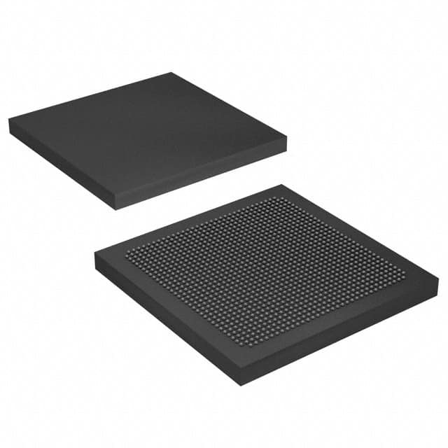
Consulte las especificaciones para obtener detalles del producto.

5SGXEA7K3F35C2LN
Basic Information Overview
- Category: Integrated Circuit (IC)
- Use: Programmable Logic Device (PLD)
- Characteristics: High-performance, low-power consumption, high-density
- Package: BGA (Ball Grid Array)
- Essence: FPGA (Field-Programmable Gate Array)
- Packaging/Quantity: Tray, 1 piece
Specifications
- Family: Stratix V
- Device: 5SGXEA7K3F35C2LN
- Logic Elements: 352,000
- Embedded Memory: 14,062 Kbits
- DSP Blocks: 3,888
- Maximum User I/O Pins: 1,280
- Operating Voltage: 0.87V - 0.97V
- Operating Temperature: -40°C to 100°C
Detailed Pin Configuration
The 5SGXEA7K3F35C2LN has a complex pin configuration with multiple pins dedicated to various functions such as input/output, clock signals, power supply, and configuration. For the detailed pin configuration, please refer to the manufacturer's datasheet.
Functional Features
- High-performance architecture for demanding applications
- Low-power consumption for energy-efficient designs
- High-density integration for complex logic designs
- Flexible and reprogrammable nature of FPGA technology
- Support for various communication protocols and interfaces
- Advanced DSP capabilities for signal processing applications
- Built-in security features for protecting intellectual property
Advantages and Disadvantages
Advantages: - Versatile and adaptable to different design requirements - Faster time-to-market due to reprogrammability - Lower development costs compared to custom ASICs - High-performance computing capabilities - Ability to implement complex algorithms and logic functions
Disadvantages: - Higher power consumption compared to specialized ASICs - Limited scalability beyond a certain level of complexity - Higher cost per unit compared to traditional microcontrollers
Working Principles
The 5SGXEA7K3F35C2LN is based on FPGA technology, which allows users to configure the device according to their specific requirements. The device consists of an array of configurable logic blocks interconnected through programmable routing resources. Users can program the device using hardware description languages (HDL) or graphical tools to define the desired functionality and interconnections between logic elements.
Detailed Application Field Plans
The 5SGXEA7K3F35C2LN is suitable for a wide range of applications, including: 1. High-performance computing systems 2. Digital signal processing (DSP) applications 3. Communication and networking equipment 4. Industrial automation and control systems 5. Video and image processing 6. Aerospace and defense systems 7. Medical imaging and diagnostics 8. Automotive electronics 9. Internet of Things (IoT) devices 10. Research and development projects
Detailed and Complete Alternative Models
- 5SGXEB7R2F40C2N: Similar features with higher logic capacity
- 5SGXEA7H2F35C2N: Lower logic capacity but lower power consumption
- 5SGXEA7K2F40C2N: Higher logic capacity with similar power consumption
- 5SGXEA7N2F45C2N: Higher logic capacity and additional features
Note: Please refer to the manufacturer's documentation for complete details and specifications of alternative models.
This entry provides an overview of the 5SGXEA7K3F35C2LN, a high-performance FPGA from the Stratix V family. It includes basic information, specifications, pin configuration, functional features, advantages and disadvantages, working principles, application field plans, and alternative models. The 5SGXEA7K3F35C2LN is a versatile and powerful programmable logic device suitable for various applications in different industries.
Enumere 10 preguntas y respuestas comunes relacionadas con la aplicación de 5SGXEA7K3F35C2LN en soluciones técnicas
Sure! Here are 10 common questions and answers related to the application of 5SGXEA7K3F35C2LN in technical solutions:
Q: What is the 5SGXEA7K3F35C2LN FPGA used for? A: The 5SGXEA7K3F35C2LN is a Field-Programmable Gate Array (FPGA) that can be used for various applications such as high-performance computing, networking, and signal processing.
Q: What are the key features of the 5SGXEA7K3F35C2LN FPGA? A: Some key features of this FPGA include a large number of logic elements, high-speed transceivers, embedded memory blocks, and support for various communication protocols.
Q: Can the 5SGXEA7K3F35C2LN FPGA be used for real-time video processing? A: Yes, the high-performance capabilities of this FPGA make it suitable for real-time video processing applications like video encoding, decoding, and image recognition.
Q: Is the 5SGXEA7K3F35C2LN FPGA suitable for high-bandwidth networking applications? A: Absolutely, this FPGA offers high-speed transceivers and support for Ethernet and other networking protocols, making it well-suited for high-bandwidth networking solutions.
Q: Can the 5SGXEA7K3F35C2LN FPGA be used in safety-critical systems? A: Yes, this FPGA supports various safety features like error correction codes (ECC), triple modular redundancy (TMR), and built-in self-test (BIST), making it suitable for safety-critical applications.
Q: Does the 5SGXEA7K3F35C2LN FPGA support PCIe connectivity? A: Yes, this FPGA supports PCIe Gen1/2/3 interfaces, enabling it to be used in applications that require high-speed data transfer over the PCIe bus.
Q: Can the 5SGXEA7K3F35C2LN FPGA be programmed using industry-standard design tools? A: Yes, this FPGA can be programmed using popular design tools like Quartus Prime from Intel, which provides a user-friendly environment for FPGA development.
Q: What is the power consumption of the 5SGXEA7K3F35C2LN FPGA? A: The power consumption of this FPGA depends on the specific application and configuration, but it typically falls within a range specified in the datasheet provided by the manufacturer.
Q: Does the 5SGXEA7K3F35C2LN FPGA support partial reconfiguration? A: Yes, this FPGA supports partial reconfiguration, allowing specific portions of the design to be modified or updated without affecting the entire system.
Q: Are there any reference designs available for the 5SGXEA7K3F35C2LN FPGA? A: Yes, the manufacturer often provides reference designs and application notes that can help developers get started with implementing the FPGA in various technical solutions.
Please note that the specific details and answers may vary based on the manufacturer's documentation and the requirements of the application.

