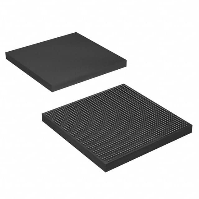
Consulte las especificaciones para obtener detalles del producto.

5SGXEA7K3F40C2N
Product Overview
Category
The 5SGXEA7K3F40C2N belongs to the category of Field-Programmable Gate Arrays (FPGAs).
Use
This FPGA is designed for high-performance applications that require complex digital logic circuits. It provides a flexible and customizable solution for various industries such as telecommunications, automotive, aerospace, and consumer electronics.
Characteristics
- High-density integration: The 5SGXEA7K3F40C2N offers a large number of programmable logic elements, allowing for the implementation of complex designs.
- High-speed performance: With advanced architecture and optimized routing resources, this FPGA can operate at high clock frequencies, enabling rapid data processing.
- Low power consumption: Despite its high performance, the 5SGXEA7K3F40C2N incorporates power-saving features, making it suitable for energy-efficient applications.
- Robust design: This FPGA is built to withstand harsh environmental conditions, ensuring reliable operation in demanding industrial settings.
Package and Quantity
The 5SGXEA7K3F40C2N is available in a compact package, typically measuring 40mm x 40mm. It is supplied in tape and reel packaging, with each reel containing a specified quantity of FPGAs.
Specifications
- Logic Elements: 358,400
- Embedded Memory: 22,671 Kbits
- DSP Blocks: 1,526
- Maximum User I/Os: 1,040
- Operating Voltage: 1.2V
- Operating Temperature Range: -40°C to 100°C
- Package Type: BGA (Ball Grid Array)
Pin Configuration
The detailed pin configuration of the 5SGXEA7K3F40C2N can be found in the manufacturer's datasheet. It provides a comprehensive overview of the pin assignments, including power supply pins, I/O pins, and configuration pins.
Functional Features
- High-speed serial transceivers: The FPGA incorporates multiple high-speed serial transceivers, enabling fast data communication between devices.
- Embedded memory blocks: The 5SGXEA7K3F40C2N includes a significant amount of embedded memory, allowing for efficient storage and retrieval of data.
- Flexible I/O interfaces: This FPGA supports various I/O standards, making it compatible with a wide range of external devices.
- Configurable logic resources: Users can program the FPGA to implement custom logic functions, providing flexibility in system design.
Advantages and Disadvantages
Advantages
- Versatility: The 5SGXEA7K3F40C2N offers a highly flexible platform that can be tailored to meet specific application requirements.
- High performance: With its advanced architecture, this FPGA delivers exceptional processing capabilities, suitable for demanding applications.
- Power efficiency: Despite its high performance, the 5SGXEA7K3F40C2N is designed to minimize power consumption, contributing to energy-efficient designs.
Disadvantages
- Complexity: Utilizing the full potential of this FPGA requires expertise in digital design and programming.
- Cost: FPGAs, including the 5SGXEA7K3F40C2N, tend to be more expensive than other integrated circuits due to their programmability and versatility.
Working Principles
The 5SGXEA7K3F40C2N operates based on the principles of reconfigurable computing. It consists of an array of programmable logic elements interconnected by configurable routing resources. By programming the FPGA, users can define the desired functionality of the circuit, which is then implemented through the interconnection of logic elements.
Application Field Plans
The 5SGXEA7K3F40C2N finds applications in various fields, including: - Telecommunications: Used in base stations, routers, and network switches to handle high-speed data processing and routing. - Automotive: Employed in advanced driver-assistance systems (ADAS) for real-time image processing and sensor fusion. - Aerospace: Utilized in satellite communication systems and onboard data processing units. - Consumer Electronics: Integrated into high-performance audio/video processing equipment and gaming consoles.
Alternative Models
For those seeking alternative options, the following FPGAs can be considered: - 5SGXEA7K2F40C2N: A similar FPGA with a slightly lower logic element count but offering comparable features. - 5SGXEA7K4F40C2N: A higher-end FPGA with increased logic elements and additional features for more demanding applications.
In conclusion, the 5SGXEA7K3F40C2N is a versatile and high-performance FPGA suitable for a wide range of applications. Its advanced features, flexibility, and robust design make it an excellent choice for complex digital circuit implementations.
Enumere 10 preguntas y respuestas comunes relacionadas con la aplicación de 5SGXEA7K3F40C2N en soluciones técnicas
Sure! Here are 10 common questions and answers related to the application of 5SGXEA7K3F40C2N in technical solutions:
Question: What is the 5SGXEA7K3F40C2N?
Answer: The 5SGXEA7K3F40C2N is a specific model of Field-Programmable Gate Array (FPGA) manufactured by Intel.Question: What are the key features of the 5SGXEA7K3F40C2N?
Answer: Some key features of this FPGA include high-performance processing capabilities, low power consumption, large capacity for logic elements, and support for various communication protocols.Question: In what technical solutions can the 5SGXEA7K3F40C2N be used?
Answer: This FPGA can be used in a wide range of applications such as telecommunications, data centers, industrial automation, aerospace, defense, and many more.Question: How does the 5SGXEA7K3F40C2N contribute to improving performance in technical solutions?
Answer: The 5SGXEA7K3F40C2N offers high-speed processing capabilities, parallel processing, and customizable hardware acceleration, which can significantly enhance the performance of various technical solutions.Question: Can the 5SGXEA7K3F40C2N be programmed or reconfigured?
Answer: Yes, the 5SGXEA7K3F40C2N is a field-programmable device, meaning it can be programmed and reconfigured to perform specific tasks based on the requirements of the technical solution.Question: What development tools are available for programming the 5SGXEA7K3F40C2N?
Answer: Intel provides Quartus Prime software, which is a comprehensive development environment for designing, simulating, and programming FPGAs like the 5SGXEA7K3F40C2N.Question: Can the 5SGXEA7K3F40C2N interface with other components or devices?
Answer: Yes, this FPGA supports various communication protocols such as PCIe, Ethernet, USB, and more, allowing it to interface with other components or devices in a technical solution.Question: What are the power requirements for the 5SGXEA7K3F40C2N?
Answer: The power requirements can vary based on the specific implementation, but generally, this FPGA operates at low power levels, making it suitable for energy-efficient solutions.Question: Are there any limitations or considerations when using the 5SGXEA7K3F40C2N?
Answer: Some considerations include the need for expertise in FPGA design, potential resource constraints depending on the complexity of the solution, and the requirement for proper cooling due to high-performance processing.Question: Where can I find additional resources or support for working with the 5SGXEA7K3F40C2N?
Answer: Intel provides documentation, application notes, reference designs, and an online community where you can find additional resources and support for working with this FPGA model.

