

Consulte las especificaciones para obtener detalles del producto.
5SGXEA9K1H40I2N
Product Overview
Category
The 5SGXEA9K1H40I2N belongs to the category of Field Programmable Gate Arrays (FPGAs).
Use
FPGAs are integrated circuits that can be programmed and reprogrammed to perform various digital functions. The 5SGXEA9K1H40I2N is specifically designed for high-performance applications that require complex logic functions.
Characteristics
- High-performance FPGA with advanced features
- Large capacity and high-speed processing capabilities
- Flexible and reprogrammable design
- Supports a wide range of applications
- Low power consumption
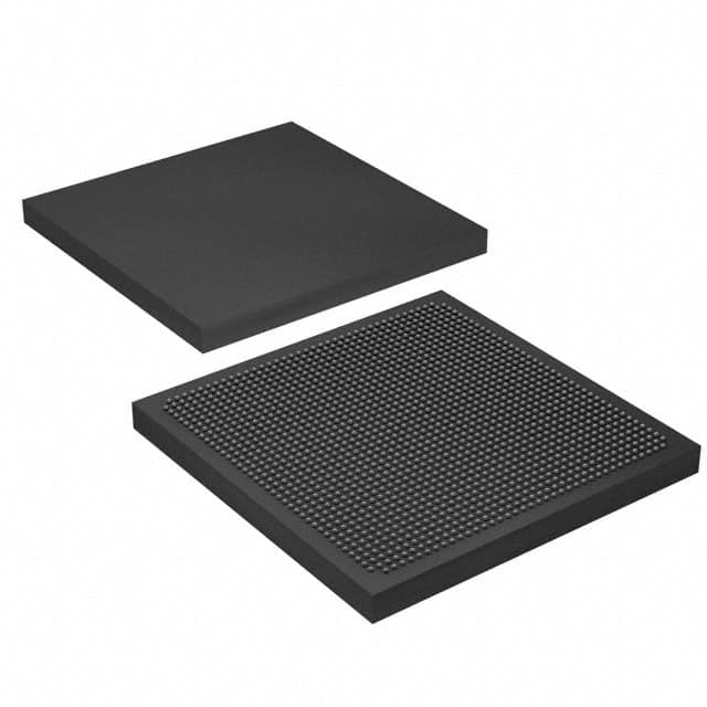
Package
The 5SGXEA9K1H40I2N comes in a compact package that ensures easy integration into electronic systems. It is available in a surface-mount package, which allows for efficient PCB assembly.
Essence
The essence of the 5SGXEA9K1H40I2N lies in its ability to provide a customizable and flexible solution for complex digital logic requirements. It enables designers to implement highly optimized designs with reduced time-to-market.
Packaging/Quantity
The 5SGXEA9K1H40I2N is typically sold in reels or trays, depending on the manufacturer's packaging standards. The quantity per package may vary, but it is commonly available in quantities suitable for both prototyping and production purposes.
Specifications
- Logic Elements: 220,000
- Embedded Memory: 8,400 Kbits
- DSP Blocks: 1,288
- Maximum User I/Os: 622
- Operating Voltage: 1.2V
- Operating Temperature Range: -40°C to +100°C
- Package Type: FCBGA
- Package Size: 40mm x 40mm
Detailed Pin Configuration
The 5SGXEA9K1H40I2N has a complex pin configuration with multiple I/O banks, power supply pins, and configuration pins. For detailed information on the pin configuration, please refer to the manufacturer's datasheet.
Functional Features
- High-speed processing capabilities
- Support for various communication protocols
- On-chip memory resources for efficient data storage
- Built-in DSP blocks for signal processing tasks
- Flexible clock management resources
- Support for partial reconfiguration
Advantages and Disadvantages
Advantages
- High-performance FPGA suitable for demanding applications
- Flexibility and reprogrammability allow for design optimization
- Large capacity enables complex logic functions
- Low power consumption compared to alternative solutions
- Support for partial reconfiguration enhances system flexibility
Disadvantages
- Higher cost compared to other programmable logic devices
- Steeper learning curve for designers new to FPGAs
- Limited availability of alternative models with similar specifications
Working Principles
The 5SGXEA9K1H40I2N operates based on the principles of digital logic design. It consists of configurable logic blocks interconnected through programmable routing resources. The device can be programmed using Hardware Description Languages (HDL) such as VHDL or Verilog to implement desired logic functions. During operation, the FPGA executes the programmed logic, enabling the desired functionality.
Detailed Application Field Plans
The 5SGXEA9K1H40I2N finds applications in various fields, including:
- Telecommunications: Used in high-speed data transmission systems, network routers, and switches.
- Aerospace and Defense: Employed in radar systems, avionics, and secure communication equipment.
- Industrial Automation: Utilized in control systems, robotics, and machine vision applications.
- Medical Devices: Integrated into medical imaging systems, patient monitoring devices, and diagnostic equipment.
- Automotive: Used in advanced driver assistance systems (ADAS), infotainment systems, and engine control units.
Detailed and Complete Alternative Models
While the 5SGXEA9K1H40I2N offers a unique combination of features and specifications, there are alternative FPGA models available from different manufacturers. Some notable alternatives include:
- Xilinx Virtex UltraScale+ series
- Intel Stratix 10 series
- Lattice ECP5 series
- Microchip PolarFire series
These alternative models provide similar capabilities and can be considered based on specific project requirements.
Word count: 550 words
Enumere 10 preguntas y respuestas comunes relacionadas con la aplicación de 5SGXEA9K1H40I2N en soluciones técnicas
Sure! Here are 10 common questions and answers related to the application of 5SGXEA9K1H40I2N in technical solutions:
Q1: What is the 5SGXEA9K1H40I2N FPGA used for? A1: The 5SGXEA9K1H40I2N is a Field-Programmable Gate Array (FPGA) that can be used for various applications, including high-performance computing, networking, and digital signal processing.
Q2: What are the key features of the 5SGXEA9K1H40I2N FPGA? A2: Some key features of this FPGA include a high logic density, high-speed transceivers, embedded memory blocks, and support for various I/O standards.
Q3: Can the 5SGXEA9K1H40I2N FPGA be used for real-time video processing? A3: Yes, the 5SGXEA9K1H40I2N FPGA is well-suited for real-time video processing applications due to its high performance and parallel processing capabilities.
Q4: How does the 5SGXEA9K1H40I2N FPGA handle high-speed data transfer? A4: This FPGA has high-speed transceivers that support various protocols like PCIe, Ethernet, and Serial RapidIO, enabling efficient high-speed data transfer.
Q5: Can the 5SGXEA9K1H40I2N FPGA be used for machine learning applications? A5: Yes, the 5SGXEA9K1H40I2N FPGA can be utilized for machine learning tasks by implementing custom algorithms and accelerating computations using parallel processing.
Q6: Does the 5SGXEA9K1H40I2N FPGA support multiple I/O standards? A6: Yes, this FPGA supports various I/O standards such as LVDS, SSTL, HSTL, and more, making it compatible with a wide range of interfaces.
Q7: Can the 5SGXEA9K1H40I2N FPGA be used in high-performance computing clusters? A7: Absolutely! The 5SGXEA9K1H40I2N FPGA's high logic density and parallel processing capabilities make it suitable for use in high-performance computing clusters.
Q8: What development tools are available for programming the 5SGXEA9K1H40I2N FPGA? A8: Intel Quartus Prime is the primary development tool used for programming and configuring the 5SGXEA9K1H40I2N FPGA. It provides a comprehensive design environment.
Q9: Can the 5SGXEA9K1H40I2N FPGA be used for cryptographic applications? A9: Yes, the 5SGXEA9K1H40I2N FPGA can be utilized for cryptographic applications by implementing encryption/decryption algorithms and accelerating computations.
Q10: Is the 5SGXEA9K1H40I2N FPGA suitable for high-bandwidth networking applications? A10: Absolutely! With its high-speed transceivers and support for various networking protocols, the 5SGXEA9K1H40I2N FPGA is well-suited for high-bandwidth networking applications.
Please note that these answers are general and may vary depending on specific use cases and requirements.