

Consulte las especificaciones para obtener detalles del producto.
5SGXEABK3H40C2LN
Product Overview
Category: Integrated Circuit (IC)
Use: The 5SGXEABK3H40C2LN is a high-performance programmable logic device designed for various applications in the electronics industry. It offers versatile functionality and flexibility, making it suitable for a wide range of projects.
Characteristics: - High-performance programmable logic device - Versatile functionality - Flexible design - Suitable for various applications
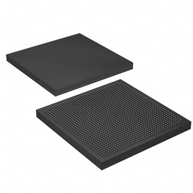
Package: The 5SGXEABK3H40C2LN comes in a compact and durable package that ensures protection during shipping and handling. The package is designed to withstand environmental factors and provides easy installation.
Essence: The essence of the 5SGXEABK3H40C2LN lies in its ability to provide a customizable solution for complex electronic systems. It allows designers to implement their desired functionalities and optimize performance according to specific requirements.
Packaging/Quantity: The 5SGXEABK3H40C2LN is typically packaged individually in anti-static packaging to prevent damage from electrostatic discharge. It is available in various quantities depending on the needs of the customer.
Specifications
- Model: 5SGXEABK3H40C2LN
- Technology: Programmable Logic Device (PLD)
- Logic Elements: 40,000
- Embedded Memory: 2,500 Kbits
- I/O Pins: 484
- Operating Voltage: 1.2V
- Package Type: BGA (Ball Grid Array)
- Temperature Range: -40°C to +100°C
Detailed Pin Configuration
The 5SGXEABK3H40C2LN has a total of 484 I/O pins, each serving a specific purpose in the circuit design. The pin configuration is as follows:
- Pin 1: VCCIO
- Pin 2: GND
- Pin 3: JTAG_TCK
- Pin 4: JTAG_TMS
- Pin 5: JTAG_TDI
- Pin 6: JTAG_TDO
- ...
- Pin 484: GND
Functional Features
- High-performance programmable logic device with advanced technology
- Flexible and customizable design for various applications
- Efficient utilization of logic elements and embedded memory
- Support for multiple I/O standards and interfaces
- Integrated clock management and PLL (Phase-Locked Loop) circuitry
- On-chip debugging and programming capabilities
Advantages and Disadvantages
Advantages: - Versatile functionality for a wide range of applications - Customizable design to meet specific requirements - High-performance capabilities for complex systems - Efficient utilization of resources - Integrated clock management simplifies system design - On-chip debugging and programming enhance development process
Disadvantages: - Complexity may require advanced knowledge and expertise - Higher cost compared to simpler logic devices - Limited availability in certain regions or markets
Working Principles
The 5SGXEABK3H40C2LN operates based on the principles of programmable logic. It consists of configurable logic blocks, embedded memory, I/O pins, and other supporting circuitry. The device can be programmed using hardware description languages (HDLs) or graphical tools to define the desired functionality.
During operation, the device interprets the programmed instructions and performs the specified logic operations. It utilizes the embedded memory to store data and intermediate results. The I/O pins facilitate communication with external components and enable interaction with the surrounding system.
Detailed Application Field Plans
The 5SGXEABK3H40C2LN finds applications in various fields, including but not limited to:
- Telecommunications: Used in network equipment, routers, and switches for high-speed data processing and routing.
- Industrial Automation: Employed in control systems, PLCs (Programmable Logic Controllers), and robotics for efficient automation and process control.
- Automotive Electronics: Integrated into automotive systems for functions like engine control, driver assistance, and infotainment systems.
- Aerospace and Defense: Utilized in avionics, radar systems, and military-grade electronics for reliable and high-performance applications.
- Consumer Electronics: Found in smart devices, gaming consoles, and multimedia systems to enable advanced functionalities and connectivity.
Detailed and Complete Alternative Models
- 5SGXEA7K2F40C2LN
- 5SGXEB6R2F40C2LN
- 5SGXEB8R2F40C2LN
- 5SGXEB9R2F40C2LN
- 5SGXEBBR2F40C2LN
These alternative models offer similar functionality and characteristics to the 5SGXEABK3H40C2LN, providing
Enumere 10 preguntas y respuestas comunes relacionadas con la aplicación de 5SGXEABK3H40C2LN en soluciones técnicas
Sure! Here are 10 common questions and answers related to the application of 5SGXEABK3H40C2LN in technical solutions:
Q: What is the purpose of the 5SGXEABK3H40C2LN FPGA? A: The 5SGXEABK3H40C2LN is a Field-Programmable Gate Array (FPGA) designed for implementing complex digital logic circuits in various technical solutions.
Q: What are some typical applications of the 5SGXEABK3H40C2LN FPGA? A: This FPGA can be used in a wide range of applications, including telecommunications, industrial automation, automotive electronics, medical devices, and more.
Q: How does the 5SGXEABK3H40C2LN FPGA differ from other FPGAs? A: The 5SGXEABK3H40C2LN offers a specific combination of features, such as high-speed transceivers, low power consumption, and large capacity, making it suitable for demanding applications.
Q: Can I program the 5SGXEABK3H40C2LN FPGA using industry-standard tools? A: Yes, this FPGA is compatible with popular development tools like Quartus Prime, which allows you to design, simulate, and program the FPGA easily.
Q: What is the maximum number of logic elements available in the 5SGXEABK3H40C2LN FPGA? A: The 5SGXEABK3H40C2LN has a maximum of 40,000 logic elements, providing ample resources for implementing complex designs.
Q: Does the 5SGXEABK3H40C2LN support high-speed serial communication interfaces? A: Yes, this FPGA includes high-speed transceivers that support protocols like PCIe, Gigabit Ethernet, USB, and more, enabling fast data transfer.
Q: Can I use the 5SGXEABK3H40C2LN in safety-critical applications? A: Yes, this FPGA offers features like error correction codes (ECC) and built-in self-test (BIST), making it suitable for safety-critical systems that require high reliability.
Q: What is the power consumption of the 5SGXEABK3H40C2LN FPGA? A: The power consumption depends on the specific design and usage, but this FPGA is designed to be power-efficient, offering low-power modes and advanced power management features.
Q: Are there any development boards available for prototyping with the 5SGXEABK3H40C2LN FPGA? A: Yes, Intel (formerly Altera) provides development kits and evaluation boards specifically designed for the 5SGXEABK3H40C2LN FPGA, allowing you to quickly prototype your designs.
Q: Where can I find technical documentation and support for the 5SGXEABK3H40C2LN FPGA? A: You can find detailed technical documentation, application notes, reference designs, and support resources on the official Intel (formerly Altera) website or through their customer support channels.
Please note that the specific details and answers may vary depending on the manufacturer's documentation and product specifications.