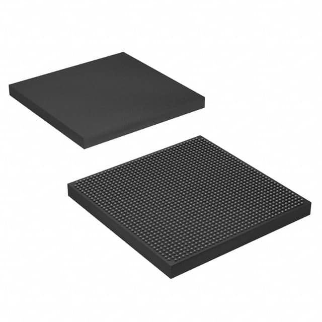
Consulte las especificaciones para obtener detalles del producto.

5SGXEB6R1F40I2N
Product Overview
Category
The 5SGXEB6R1F40I2N belongs to the category of Field Programmable Gate Arrays (FPGAs).
Use
FPGAs are integrated circuits that can be programmed and reprogrammed to perform various digital functions. The 5SGXEB6R1F40I2N is specifically designed for high-performance applications.
Characteristics
- High-performance FPGA with advanced features
- Large capacity and high-speed processing capabilities
- Flexible and reconfigurable design
- Low power consumption
- Robust and reliable performance
Package
The 5SGXEB6R1F40I2N comes in a compact package, suitable for integration into electronic systems.
Essence
The essence of the 5SGXEB6R1F40I2N lies in its ability to provide a customizable and high-performance solution for complex digital designs.
Packaging/Quantity
The 5SGXEB6R1F40I2N is typically packaged individually and is available in various quantities depending on the customer's requirements.
Specifications
- FPGA Family: Stratix V
- Logic Elements: 622,080
- Embedded Memory: 34,816 Kbits
- DSP Blocks: 3,888
- Maximum User I/Os: 1,280
- Operating Voltage: 1.0V
- Operating Temperature Range: -40°C to +100°C
Detailed Pin Configuration
The 5SGXEB6R1F40I2N has a comprehensive pin configuration, allowing for connectivity with other components and external devices. Please refer to the datasheet for the detailed pinout information.
Functional Features
- High-speed data processing capabilities
- Support for various communication protocols
- On-chip memory for efficient data storage
- Flexible I/O interfaces for seamless integration
- Advanced clock management and synchronization features
Advantages and Disadvantages
Advantages
- High-performance computing capabilities
- Flexibility in design and reconfiguration
- Low power consumption compared to alternative solutions
- Extensive range of I/O options for connectivity
- Reliable and robust operation
Disadvantages
- Higher cost compared to traditional microcontrollers
- Steeper learning curve for programming and utilization
- Limited availability of specialized technical support
Working Principles
The 5SGXEB6R1F40I2N operates based on the principles of digital logic. It consists of a network of configurable logic blocks, interconnected by programmable routing resources. The user can program the FPGA to implement specific digital functions by configuring the interconnections and functionality of these logic blocks.
Detailed Application Field Plans
The 5SGXEB6R1F40I2N finds applications in various fields that require high-performance digital processing. Some potential application areas include:
- Telecommunications: FPGAs are used in base stations, routers, and network switches to handle high-speed data processing and communication protocols.
- Aerospace and Defense: FPGAs are utilized in radar systems, avionics, and military communication equipment for their reliability and performance.
- Industrial Automation: FPGAs enable real-time control and monitoring in industrial automation systems, improving efficiency and accuracy.
- Medical Devices: FPGAs are employed in medical imaging, patient monitoring, and diagnostic equipment for their computational power and flexibility.
- Research and Development: FPGAs serve as a versatile platform for prototyping and testing new digital designs in various research fields.
Detailed and Complete Alternative Models
- Xilinx Virtex UltraScale+ VU9P: Another high-performance FPGA with advanced features and large capacity.
- Intel Cyclone 10 GX: A cost-effective FPGA solution suitable for mid-range applications.
- Lattice ECP5: A low-power FPGA with excellent performance-per-watt ratio, ideal for battery-powered devices.
These alternative models offer different features and price points, allowing users to choose the most suitable FPGA for their specific requirements.
Word count: 550 words
Enumere 10 preguntas y respuestas comunes relacionadas con la aplicación de 5SGXEB6R1F40I2N en soluciones técnicas
Sure! Here are 10 common questions and answers related to the application of 5SGXEB6R1F40I2N in technical solutions:
Q1: What is the 5SGXEB6R1F40I2N FPGA used for? A1: The 5SGXEB6R1F40I2N FPGA is commonly used for high-performance applications that require programmable logic, such as data processing, image and video processing, networking, and industrial automation.
Q2: What are the key features of the 5SGXEB6R1F40I2N FPGA? A2: The key features of the 5SGXEB6R1F40I2N FPGA include a large number of logic elements, high-speed transceivers, embedded memory blocks, DSP blocks, and support for various communication protocols.
Q3: How can I program the 5SGXEB6R1F40I2N FPGA? A3: The 5SGXEB6R1F40I2N FPGA can be programmed using hardware description languages (HDLs) like Verilog or VHDL. You can use development tools provided by the FPGA manufacturer, such as Quartus Prime, to write, compile, and program the FPGA.
Q4: Can the 5SGXEB6R1F40I2N FPGA interface with other components or devices? A4: Yes, the 5SGXEB6R1F40I2N FPGA supports various interfaces like PCIe, Ethernet, USB, DDR3/DDR4 memory, and more. It can easily interface with other components or devices in your system.
Q5: What kind of performance can I expect from the 5SGXEB6R1F40I2N FPGA? A5: The performance of the 5SGXEB6R1F40I2N FPGA depends on the specific application and design implementation. However, it offers high-speed transceivers, large logic capacity, and dedicated DSP blocks, enabling high-performance processing capabilities.
Q6: Can I reprogram the 5SGXEB6R1F40I2N FPGA after deployment? A6: Yes, the 5SGXEB6R1F40I2N FPGA is reprogrammable, allowing you to update or modify the functionality of your design even after deployment. This flexibility is one of the key advantages of using FPGAs.
Q7: Are there any development boards available for the 5SGXEB6R1F40I2N FPGA? A7: Yes, the manufacturer provides development boards that are specifically designed for the 5SGXEB6R1F40I2N FPGA. These boards come with various interfaces, connectors, and peripherals to aid in the development and testing of your designs.
Q8: What kind of power requirements does the 5SGXEB6R1F40I2N FPGA have? A8: The power requirements of the 5SGXEB6R1F40I2N FPGA depend on the specific configuration and usage. It typically requires multiple power supply rails, including core voltage and I/O voltage, which can be found in the device datasheet.
Q9: Can the 5SGXEB6R1F40I2N FPGA be used in safety-critical applications? A9: Yes, the 5SGXEB6R1F40I2N FPGA can be used in safety-critical applications. However, it is important to follow proper design practices, such as redundancy, fault tolerance, and rigorous testing, to ensure the reliability and safety of the overall system.
Q10: Where can I find technical documentation and support for the 5SGXEB6R1F40I2N FPGA? A10: You can find technical documentation, datasheets, reference designs, and application notes on the manufacturer's website. Additionally, the manufacturer usually provides technical support through forums, online communities, and direct contact with their support team.

