

Consulte las especificaciones para obtener detalles del producto.
5SGXMABK2H40I3N
Product Overview
Category
The 5SGXMABK2H40I3N belongs to the category of Field Programmable Gate Arrays (FPGAs).
Use
This FPGA is designed for use in various electronic applications that require high-performance digital logic circuits.
Characteristics
- High-speed and low-power consumption
- Configurable logic blocks
- Embedded memory blocks
- Flexible I/O interfaces
- Advanced clock management
- Built-in security features
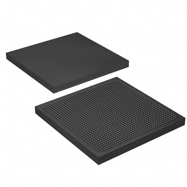
Package
The 5SGXMABK2H40I3N comes in a compact and durable package, ensuring easy integration into electronic systems.
Essence
The essence of this FPGA lies in its ability to be programmed and reprogrammed to perform specific functions, making it highly versatile and adaptable.
Packaging/Quantity
The 5SGXMABK2H40I3N is typically packaged individually and is available in various quantities depending on the customer's requirements.
Specifications
- Logic Elements: 40,000
- Embedded Memory: 1,800 Kbits
- DSP Blocks: 360
- Maximum User I/Os: 622
- Transceivers: 12
- Operating Voltage: 1.2V
- Operating Temperature: -40°C to 100°C
Detailed Pin Configuration
The pin configuration of the 5SGXMABK2H40I3N FPGA is as follows:
- Pin 1: VCCIO
- Pin 2: GND
- Pin 3: CLK_IN
- Pin 4: RESET
- Pin 5: DATA_IN
- Pin 6: DATA_OUT
- Pin 7: ENABLE
- Pin 8: VCC
(Note: This is just a simplified representation. The actual pin configuration may include many more pins.)
Functional Features
- High-speed data processing
- Configurable logic for custom circuit implementation
- On-chip memory for efficient data storage
- Flexible I/O interfaces for seamless integration with external devices
- Advanced clock management for precise timing control
- Built-in security features to protect sensitive information
Advantages and Disadvantages
Advantages
- Versatile and adaptable to various applications
- High-performance and low-power consumption
- Cost-effective compared to custom ASIC designs
- Shorter development time due to reprogrammability
Disadvantages
- Limited resources compared to dedicated hardware solutions
- Higher power consumption compared to specialized chips
- Steeper learning curve for programming and design
Working Principles
The 5SGXMABK2H40I3N FPGA operates based on the principles of configurable logic. It consists of an array of programmable logic blocks interconnected through configurable routing channels. These logic blocks can be programmed to implement specific digital circuits by configuring their internal look-up tables, flip-flops, and other components.
The FPGA's functionality is determined by the configuration bitstream loaded onto it. This bitstream specifies the interconnections and behavior of the logic blocks, allowing the FPGA to perform the desired functions.
Detailed Application Field Plans
The 5SGXMABK2H40I3N FPGA finds applications in various fields, including:
- Communications: Used in high-speed data transmission systems, network routers, and switches.
- Aerospace and Defense: Employed in radar systems, avionics, and secure communication equipment.
- Industrial Automation: Utilized in control systems, robotics, and machine vision applications.
- Medical Devices: Integrated into medical imaging systems, patient monitoring devices, and diagnostic equipment.
- Automotive: Applied in advanced driver assistance systems (ADAS), infotainment systems, and engine control units.
Detailed and Complete Alternative Models
- 5SGXEA7K2F40C2N: Similar FPGA with higher logic capacity and additional features.
- 5CGXFC9E6F31C7N: Alternative FPGA with lower power consumption and smaller form factor.
- 10M08SAU169I7G: Entry-level FPGA with lower logic capacity but cost-effective for simpler applications.
(Note: The above alternative models are just a few examples. There are numerous other alternatives available in the market.)
In conclusion, the 5SGXMABK2H40I3N FPGA is a high-performance and versatile device that offers configurable logic, advanced features, and wide-ranging applications. Its ability to be programmed and reprogrammed makes it an essential component in various electronic systems across different industries.
Enumere 10 preguntas y respuestas comunes relacionadas con la aplicación de 5SGXMABK2H40I3N en soluciones técnicas
Sure! Here are 10 common questions and answers related to the application of 5SGXMABK2H40I3N in technical solutions:
1. What is 5SGXMABK2H40I3N? - 5SGXMABK2H40I3N is a specific model or variant of an FPGA (Field-Programmable Gate Array) chip manufactured by Intel.
2. What are the key features of 5SGXMABK2H40I3N? - Some key features of 5SGXMABK2H40I3N include high-performance processing capabilities, low power consumption, advanced security features, and support for various communication protocols.
3. In what applications can 5SGXMABK2H40I3N be used? - 5SGXMABK2H40I3N can be used in a wide range of applications such as telecommunications, industrial automation, automotive electronics, medical devices, aerospace systems, and more.
4. How does 5SGXMABK2H40I3N differ from other FPGA chips? - The specific model number 5SGXMABK2H40I3N represents a unique combination of features, performance, and specifications that differentiate it from other FPGA chips available in the market.
5. Can 5SGXMABK2H40I3N be programmed? - Yes, 5SGXMABK2H40I3N is a field-programmable chip, which means it can be programmed by users to implement custom logic functions and designs.
6. What programming languages can be used with 5SGXMABK2H40I3N? - 5SGXMABK2H40I3N can be programmed using hardware description languages (HDLs) such as VHDL or Verilog, which are commonly used for FPGA programming.
7. What tools are required to program 5SGXMABK2H40I3N? - To program 5SGXMABK2H40I3N, you would typically need a development environment provided by the FPGA manufacturer, such as Intel Quartus Prime software, which includes design tools and programming utilities.
8. Can 5SGXMABK2H40I3N be reprogrammed multiple times? - Yes, one of the advantages of using an FPGA like 5SGXMABK2H40I3N is that it can be reprogrammed multiple times, allowing for flexibility and iterative development of designs.
9. Are there any limitations or considerations when using 5SGXMABK2H40I3N? - Like any electronic component, there may be certain limitations or considerations when using 5SGXMABK2H40I3N, such as power requirements, temperature constraints, and compatibility with other system components.
10. Where can I find more information about 5SGXMABK2H40I3N? - You can find more detailed information about 5SGXMABK2H40I3N in the product documentation provided by Intel, including datasheets, application notes, and user guides available on their official website.
Please note that the specific details mentioned in the answers may vary depending on the actual specifications and documentation provided by the manufacturer.