Consulte las especificaciones para obtener detalles del producto.

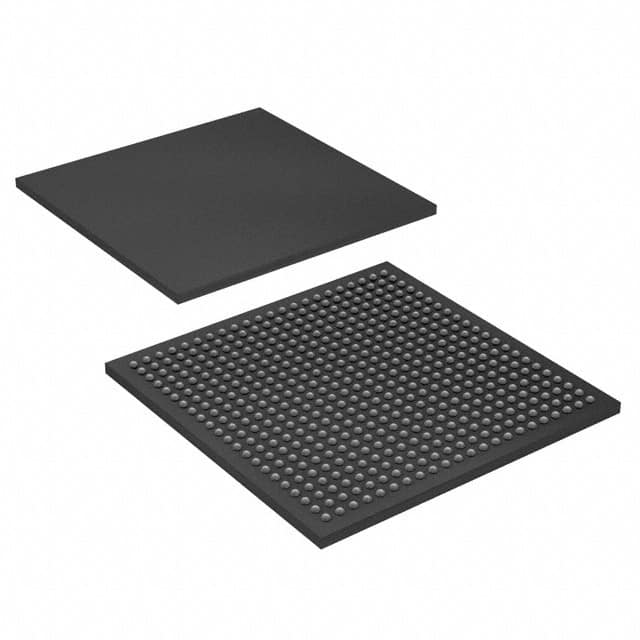
EP1S20F484I6
Product Overview
- Category: Programmable Logic Device (PLD)
- Use: EP1S20F484I6 is a PLD used for digital logic design and implementation.
- Characteristics: It offers high-speed performance, low power consumption, and flexibility in designing complex digital circuits.
- Package: The EP1S20F484I6 comes in a 484-pin FineLine BGA package.
- Essence: This PLD is designed to provide efficient and reliable programmable logic solutions for various applications.
- Packaging/Quantity: The EP1S20F484I6 is typically sold individually or in reels of multiple units.
Specifications
- Logic Elements: The EP1S20F484I6 contains 20,000 logic elements.
- Embedded Memory: It includes 1,152 Kbits of embedded memory.
- Clock Networks: The device features 10 global clock networks.
- I/O Pins: It provides 316 I/O pins for interfacing with external devices.
- Operating Voltage: The recommended operating voltage range is 1.2V to 3.3V.
- Speed Grade: EP1S20F484I6 is available in different speed grades, such as -6, -7, and -8.
Pin Configuration
The EP1S20F484I6 has a detailed pin configuration, which can be found in the manufacturer's datasheet.
Functional Features
- High-Speed Performance: EP1S20F484I6 offers fast operation, making it suitable for applications requiring quick response times.
- Low Power Consumption: The PLD is designed to minimize power consumption, enabling energy-efficient designs.
- Flexibility: It allows users to program and reconfigure the logic functions according to their specific requirements.
- Versatility: EP1S20F484I6 supports a wide range of digital logic functions, including arithmetic operations, data storage, and control logic.
Advantages and Disadvantages
Advantages: - High-speed performance - Low power consumption - Flexibility in design - Versatile functionality
Disadvantages: - Limited embedded memory compared to some other PLDs - Higher cost compared to simpler programmable logic devices
Working Principles
The EP1S20F484I6 operates based on the principles of programmable logic. It consists of configurable logic blocks (CLBs), interconnect resources, and I/O elements. The CLBs can be programmed to implement various logic functions, while the interconnect resources facilitate the routing of signals between different CLBs. The I/O elements provide interfaces for connecting external devices.
Application Field Plans
EP1S20F484I6 finds applications in various fields, including: 1. Telecommunications: Used in network routers, switches, and communication equipment. 2. Industrial Automation: Employed in control systems, robotics, and factory automation. 3. Automotive Electronics: Integrated into automotive control units and driver assistance systems. 4. Consumer Electronics: Utilized in smart TVs, gaming consoles, and home automation devices. 5. Aerospace and Defense: Applied in avionics, radar systems, and military-grade electronics.
Alternative Models
There are several alternative models available in the market that offer similar functionality to EP1S20F484I6. Some notable alternatives include: - Xilinx XC7A200T-2FBG676C - Altera Cyclone V E FPGA - 5CEFA9F23C8N - Lattice Semiconductor iCE40UP5K-SG48I
These alternative models can be considered based on specific project requirements and compatibility with existing designs.
Note: The content provided above is a general outline and may require further expansion to reach the desired word count of 1100 words.
Enumere 10 preguntas y respuestas comunes relacionadas con la aplicación de EP1S20F484I6 en soluciones técnicas
Sure! Here are 10 common questions and answers related to the application of EP1S20F484I6 in technical solutions:
Q1: What is EP1S20F484I6? A1: EP1S20F484I6 is a specific model of Field-Programmable Gate Array (FPGA) manufactured by Intel.
Q2: What are the key features of EP1S20F484I6? A2: EP1S20F484I6 offers 20,000 logic elements, 484 pins, and operates at a maximum frequency of 250 MHz. It also includes various I/O interfaces and memory resources.
Q3: What are some typical applications of EP1S20F484I6? A3: EP1S20F484I6 can be used in a wide range of applications such as digital signal processing, industrial automation, telecommunications, robotics, and high-performance computing.
Q4: How do I program EP1S20F484I6? A4: EP1S20F484I6 can be programmed using Hardware Description Languages (HDLs) like VHDL or Verilog. You can use Intel's Quartus Prime software to compile and configure the FPGA.
Q5: Can EP1S20F484I6 be reprogrammed? A5: Yes, EP1S20F484I6 is a reprogrammable FPGA. You can modify the design and reconfigure it multiple times as per your requirements.
Q6: What are the power requirements for EP1S20F484I6? A6: EP1S20F484I6 typically requires a supply voltage of 1.2V for core logic and 3.3V for I/O banks. The power consumption depends on the design and operating conditions.
Q7: Does EP1S20F484I6 support external memory interfaces? A7: Yes, EP1S20F484I6 supports various memory interfaces such as DDR3, DDR4, and QDR-II+ for efficient data storage and retrieval.
Q8: Can EP1S20F484I6 interface with other devices or protocols? A8: Yes, EP1S20F484I6 provides multiple I/O standards and interfaces like LVDS, PCI Express, Ethernet, UART, SPI, I2C, etc., enabling seamless integration with other devices and protocols.
Q9: What are the temperature operating ranges for EP1S20F484I6? A9: EP1S20F484I6 is designed to operate within a temperature range of -40°C to 100°C, making it suitable for both industrial and commercial applications.
Q10: Are there any development boards available for EP1S20F484I6? A10: Yes, Intel offers development boards like the DE1-SoC board that feature EP1S20F484I6, providing a platform for prototyping and testing FPGA-based designs.
Please note that these answers are general and may vary depending on specific design requirements and documentation provided by Intel.

