

Consulte las especificaciones para obtener detalles del producto.
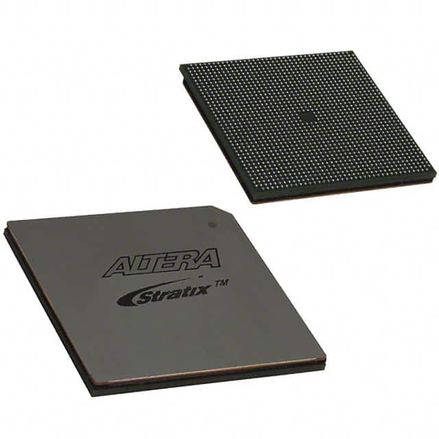
EP1S40F1508C7N
Basic Information Overview
- Category: Integrated Circuit (IC)
- Use: Programmable Logic Device (PLD)
- Characteristics: High-performance, low-power consumption, reprogrammable
- Package: 1508-ball FineLine BGA package
- Essence: A versatile PLD for various digital logic applications
- Packaging/Quantity: Typically sold in reels or trays containing multiple units
Specifications
- Technology: Field-Programmable Gate Array (FPGA)
- Logic Elements: 40,000
- Speed Grade: C7
- I/O Pins: 1508
- Operating Voltage: 1.2V
- Operating Temperature: -40°C to 100°C
- Package Dimensions: 35mm x 35mm
Detailed Pin Configuration
The EP1S40F1508C7N has a complex pin configuration with 1508 pins. For the detailed pinout diagram and description, please refer to the datasheet provided by the manufacturer.
Functional Features
- High-density integration of programmable logic elements
- Flexible and reprogrammable design allows for customization
- Support for various communication protocols and interfaces
- Advanced clock management and synchronization capabilities
- On-chip memory blocks for efficient data storage
- Built-in security features to protect intellectual property
Advantages and Disadvantages
Advantages: - Versatile and adaptable for different applications - High-performance and low-power consumption - Reprogrammable nature allows for design iterations - Large number of I/O pins for extensive connectivity options
Disadvantages: - Complex pin configuration may require careful planning - Initial learning curve for programming and utilization - Higher cost compared to fixed-function integrated circuits
Working Principles
The EP1S40F1508C7N is based on FPGA technology, which utilizes a matrix of configurable logic blocks and programmable interconnects. The device can be programmed to implement various digital logic functions, such as combinational and sequential circuits, arithmetic operations, and memory structures. The configuration data is stored in on-chip memory elements and can be modified by the user. During operation, the FPGA dynamically routes signals through the programmable interconnects to achieve the desired functionality.
Detailed Application Field Plans
The EP1S40F1508C7N finds applications in a wide range of fields, including: - Telecommunications: Baseband processing, network routers, protocol converters - Industrial Automation: Control systems, motor drives, sensor interfaces - Automotive: Advanced driver-assistance systems (ADAS), infotainment systems - Aerospace and Defense: Radar signal processing, avionics, secure communication - Consumer Electronics: High-definition video processing, gaming consoles, smart appliances
Detailed and Complete Alternative Models
- EP1S30F780C6N: Smaller capacity FPGA with 30,000 logic elements and 780 I/O pins
- EP1S60F1020C5N: Higher capacity FPGA with 60,000 logic elements and 1020 I/O pins
- EP2S180F1508C4N: FPGA with larger capacity and lower power consumption
Note: Please refer to the manufacturer's documentation for complete details on alternative models.
This entry provides an overview of the EP1S40F1508C7N, a versatile programmable logic device used in various digital logic applications. It includes basic information, specifications, pin configuration, functional features, advantages and disadvantages, working principles, application field plans, and alternative models.
Enumere 10 preguntas y respuestas comunes relacionadas con la aplicación de EP1S40F1508C7N en soluciones técnicas
Sure! Here are 10 common questions and answers related to the application of EP1S40F1508C7N in technical solutions:
Q1: What is EP1S40F1508C7N? A1: EP1S40F1508C7N is a specific model of Field Programmable Gate Array (FPGA) manufactured by Intel.
Q2: What are the key features of EP1S40F1508C7N? A2: Some key features of EP1S40F1508C7N include 40,000 logic elements, 1.5V core voltage, and support for various I/O standards.
Q3: What are the typical applications of EP1S40F1508C7N? A3: EP1S40F1508C7N is commonly used in applications such as telecommunications, industrial automation, automotive electronics, and high-performance computing.
Q4: How can EP1S40F1508C7N be programmed? A4: EP1S40F1508C7N can be programmed using hardware description languages (HDLs) like VHDL or Verilog, which allow designers to describe the desired functionality of the FPGA.
Q5: Can EP1S40F1508C7N be reprogrammed after initial programming? A5: Yes, EP1S40F1508C7N is a field-programmable device, meaning it can be reprogrammed multiple times to implement different functionalities.
Q6: What tools are available for programming EP1S40F1508C7N? A6: Intel provides Quartus Prime software, which includes a suite of tools for designing, simulating, and programming EP1S40F1508C7N FPGAs.
Q7: What is the power consumption of EP1S40F1508C7N? A7: The power consumption of EP1S40F1508C7N depends on the specific design and operating conditions, but it typically ranges from a few watts to tens of watts.
Q8: Can EP1S40F1508C7N interface with other components or devices? A8: Yes, EP1S40F1508C7N supports various I/O standards, allowing it to interface with different components and devices such as sensors, memory modules, and communication interfaces.
Q9: Are there any limitations or considerations when using EP1S40F1508C7N? A9: Some considerations include power supply requirements, thermal management, and ensuring proper signal integrity in high-speed designs. Referring to the datasheet and application notes is recommended.
Q10: Where can I find additional resources and support for EP1S40F1508C7N? A10: Intel provides documentation, reference designs, forums, and technical support on their website to assist users in working with EP1S40F1508C7N.
Please note that the answers provided here are general and may vary depending on specific requirements and use cases.