

Consulte las especificaciones para obtener detalles del producto.
EP3C10E144C7
Product Overview
Category
EP3C10E144C7 belongs to the category of programmable logic devices (PLDs).
Use
This product is used for implementing digital circuits and systems in various applications.
Characteristics
- EP3C10E144C7 is a low-cost, low-power PLD.
- It offers high performance and flexibility in designing complex digital systems.
- The device supports reprogrammability, allowing for easy modifications and updates.
- It has a compact package, making it suitable for space-constrained designs.
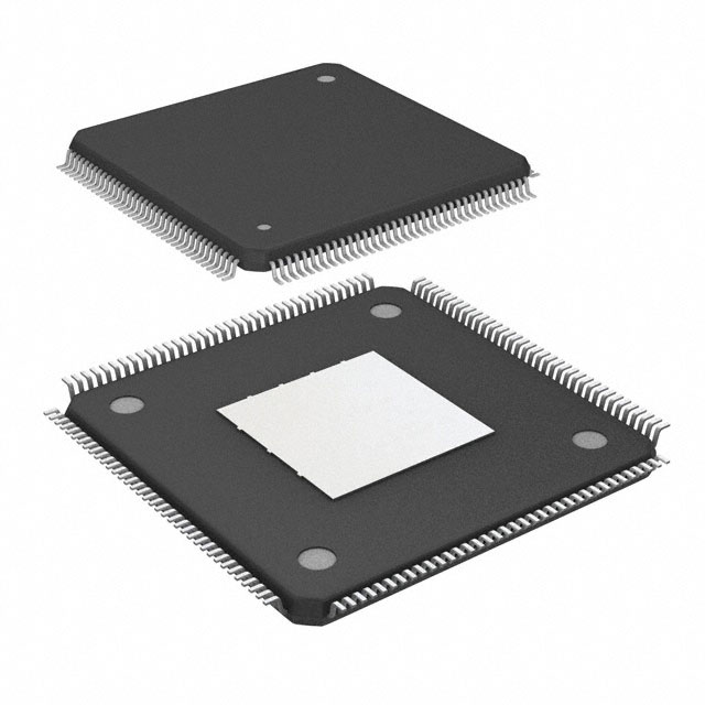
Package
EP3C10E144C7 is available in a 144-pin quad flat pack (QFP) package.
Essence
The essence of EP3C10E144C7 lies in its ability to provide a customizable and cost-effective solution for digital circuit implementation.
Packaging/Quantity
This product is typically sold individually or in small quantities, depending on the supplier.
Specifications
- Logic elements: 10,080
- RAM bits: 414,720
- Maximum user I/Os: 101
- Clock management tiles: 4
- PLLs: 2
- Maximum user flash memory: 270,336 bits
- Operating voltage: 1.2V
- Speed grade: C7
Detailed Pin Configuration
The pin configuration of EP3C10E144C7 can be found in the datasheet provided by the manufacturer. It includes information about the functions and connections of each pin.
Functional Features
- High-density programmable logic with abundant logic elements and memory resources.
- Flexible I/O options for interfacing with external devices.
- Dedicated clock management tiles for precise timing control.
- On-chip phase-locked loops (PLLs) for generating stable clock signals.
- Flash memory for storing configuration data.
- JTAG interface for programming and debugging.
Advantages and Disadvantages
Advantages
- Cost-effective solution for implementing digital circuits.
- High flexibility and reprogrammability.
- Compact package suitable for space-constrained designs.
- Abundant logic elements and memory resources.
Disadvantages
- Limited I/O options compared to larger PLDs.
- May require additional components for certain applications.
- Steeper learning curve for beginners due to the complexity of programmable logic devices.
Working Principles
EP3C10E144C7 is based on field-programmable gate array (FPGA) technology. It consists of configurable logic blocks, memory elements, and interconnects. The device can be programmed using hardware description languages (HDLs) or graphical design tools. Once programmed, the FPGA implements the desired digital circuit by configuring its internal resources.
Detailed Application Field Plans
EP3C10E144C7 finds applications in various fields, including: - Industrial automation - Communications systems - Consumer electronics - Automotive electronics - Medical devices - Aerospace and defense
The device can be used to implement functions such as data processing, signal conditioning, control logic, and interface protocols in these application areas.
Detailed and Complete Alternative Models
Some alternative models to EP3C10E144C7 include: - EP3C16E144C8: Higher logic capacity and more I/O options. - EP3C25E144C8: Increased logic elements and memory resources. - EP4CE6E22C8N: Enhanced performance and higher speed grade.
These alternative models offer different features and capabilities, allowing designers to choose the most suitable option for their specific requirements.
Word count: 515 words
Enumere 10 preguntas y respuestas comunes relacionadas con la aplicación de EP3C10E144C7 en soluciones técnicas
Sure! Here are 10 common questions and answers related to the application of EP3C10E144C7 in technical solutions:
Q: What is EP3C10E144C7? A: EP3C10E144C7 is a specific model of Field-Programmable Gate Array (FPGA) manufactured by Intel (formerly Altera). It offers 10,000 logic elements and comes in a 144-pin package.
Q: What are the typical applications of EP3C10E144C7? A: EP3C10E144C7 can be used in various technical solutions such as industrial automation, robotics, telecommunications, medical devices, automotive systems, and more.
Q: How does EP3C10E144C7 differ from other FPGAs? A: EP3C10E144C7 stands out for its compact size, low power consumption, and cost-effectiveness while still providing a decent number of logic elements for many applications.
Q: Can EP3C10E144C7 handle complex algorithms and computations? A: Yes, EP3C10E144C7 is capable of handling complex algorithms and computations due to its programmable nature, allowing users to implement custom logic designs.
Q: What development tools are available for programming EP3C10E144C7? A: Intel Quartus Prime is the primary development tool used for programming EP3C10E144C7. It provides a comprehensive environment for designing, simulating, and programming FPGA designs.
Q: Can EP3C10E144C7 interface with other components or devices? A: Yes, EP3C10E144C7 supports various communication protocols such as I2C, SPI, UART, and GPIO, allowing it to interface with other components or devices in a system.
Q: Is EP3C10E144C7 suitable for real-time applications? A: Yes, EP3C10E144C7 can be used in real-time applications as it offers fast processing speeds and low-latency capabilities when properly designed and programmed.
Q: Can EP3C10E144C7 be reprogrammed after deployment? A: Yes, EP3C10E144C7 is a reprogrammable FPGA, which means that its configuration can be updated or changed even after it has been deployed in a system.
Q: Are there any limitations to using EP3C10E144C7? A: EP3C10E144C7 has a limited number of logic elements compared to higher-end FPGAs, so it may not be suitable for extremely complex designs requiring a large number of resources.
Q: Where can I find more information about EP3C10E144C7? A: You can refer to the official documentation provided by Intel (formerly Altera) for detailed specifications, application notes, reference designs, and user guides related to EP3C10E144C7.