

Consulte las especificaciones para obtener detalles del producto.
EP4CE15E22C7
Product Overview
- Category: Programmable Logic Device (PLD)
- Use: EP4CE15E22C7 is a PLD used for digital logic applications.
- Characteristics: It offers high performance, low power consumption, and flexibility in design.
- Package: The EP4CE15E22C7 comes in a compact package suitable for integration into various electronic systems.
- Essence: This PLD provides a versatile solution for implementing complex digital logic functions.
- Packaging/Quantity: The EP4CE15E22C7 is typically sold in trays or reels, with quantities varying based on customer requirements.
Specifications
- Logic Elements: 15,183
- Embedded Memory: 414 Kbits
- Maximum User I/O Pins: 179
- Maximum User Flash Memory: 2,208 Kbits
- Clock Networks: 8
- PLLs: 2
- Maximum Operating Frequency: 300 MHz
- Voltage Range: 1.14V to 1.26V
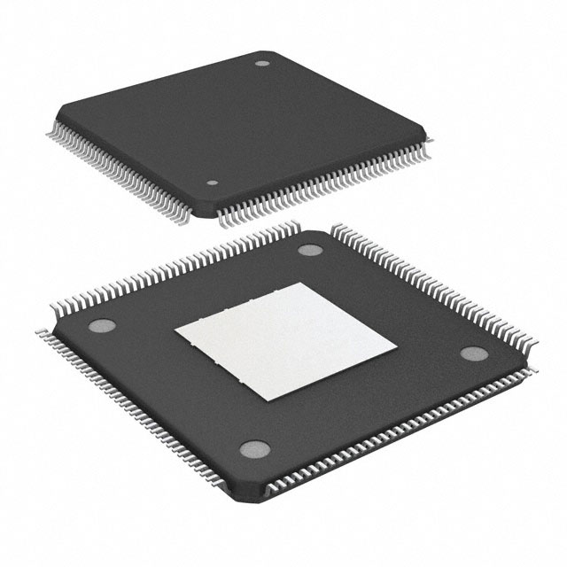
Detailed Pin Configuration
The EP4CE15E22C7 has a total of 179 user I/O pins, which can be configured as inputs or outputs based on the application requirements. These pins are distributed across the device and provide connectivity to external components.
For a detailed pin configuration diagram, please refer to the official datasheet provided by the manufacturer.
Functional Features
- High-performance architecture allows for efficient implementation of complex digital logic functions.
- Low power consumption enables energy-efficient operation.
- Flexible design options provide customization possibilities for various applications.
- Integrated memory blocks facilitate data storage and retrieval operations.
- Multiple clock networks and PLLs enable precise timing control.
Advantages and Disadvantages
Advantages: - High performance and flexibility in design. - Low power consumption. - Integrated memory blocks for efficient data handling. - Precise timing control with multiple clock networks and PLLs.
Disadvantages: - Limited number of user I/O pins. - Higher cost compared to simpler programmable logic devices. - Steeper learning curve for beginners due to its complexity.
Working Principles
The EP4CE15E22C7 is based on a field-programmable gate array (FPGA) architecture. It consists of configurable logic blocks (CLBs), interconnect resources, embedded memory blocks, and other essential components. The CLBs can be programmed to implement various digital logic functions, allowing users to create custom designs.
The device's configuration is stored in non-volatile memory, which is loaded during power-up. Once configured, the EP4CE15E22C7 operates according to the programmed logic, processing input signals and generating desired output signals.
Detailed Application Field Plans
The EP4CE15E22C7 finds applications in various fields, including:
- Communications: Used in networking equipment, routers, and switches for data processing and protocol handling.
- Industrial Automation: Employed in control systems, robotics, and machine vision applications for real-time processing and control.
- Automotive: Integrated into automotive electronics for functions like engine management, advanced driver-assistance systems (ADAS), and infotainment systems.
- Aerospace: Utilized in avionics systems for flight control, navigation, and communication.
- Consumer Electronics: Found in smart TVs, gaming consoles, and wearable devices for high-performance computing and multimedia processing.
Detailed and Complete Alternative Models
- EP4CE6E22C8: A smaller variant with 6,183 logic elements and 208 Kbits of embedded memory.
- EP4CE10E22C8: Offers intermediate capacity with 10,183 logic elements and 332 Kbits of embedded memory.
- EP4CE30E22C8: A higher-end model with 30,183 logic elements and 1,248 Kbits of embedded memory.
These alternative models provide options for different project requirements, offering varying levels of logic capacity and memory resources.
Word count: 482 words
Enumere 10 preguntas y respuestas comunes relacionadas con la aplicación de EP4CE15E22C7 en soluciones técnicas
Sure! Here are 10 common questions and answers related to the application of EP4CE15E22C7 in technical solutions:
Q: What is EP4CE15E22C7? A: EP4CE15E22C7 is a field-programmable gate array (FPGA) chip manufactured by Intel (formerly Altera). It offers programmable logic, memory, and digital signal processing capabilities.
Q: What are some typical applications of EP4CE15E22C7? A: EP4CE15E22C7 can be used in various technical solutions such as industrial automation, robotics, telecommunications, automotive electronics, medical devices, and more.
Q: How does EP4CE15E22C7 differ from other FPGA chips? A: EP4CE15E22C7 has specific features like 15,408 logic elements, 414,720 bits of embedded memory, and 266 multipliers that differentiate it from other FPGA chips.
Q: Can EP4CE15E22C7 be programmed using popular hardware description languages (HDLs)? A: Yes, EP4CE15E22C7 can be programmed using HDLs like VHDL or Verilog, which are widely used in the FPGA design community.
Q: Is EP4CE15E22C7 suitable for high-speed data processing applications? A: Yes, EP4CE15E22C7 supports high-speed serial transceivers, making it suitable for applications requiring fast data processing and communication.
Q: Can EP4CE15E22C7 interface with external devices? A: Yes, EP4CE15E22C7 has various I/O pins that allow it to interface with external devices such as sensors, actuators, displays, and communication modules.
Q: Does EP4CE15E22C7 support real-time processing? A: Yes, EP4CE15E22C7 can be programmed to perform real-time processing tasks by implementing dedicated hardware accelerators or using its embedded processors.
Q: Can EP4CE15E22C7 be reprogrammed after deployment? A: Yes, EP4CE15E22C7 is a field-programmable device, meaning it can be reprogrammed even after it has been deployed in a system.
Q: Are there any development tools available for programming EP4CE15E22C7? A: Yes, Intel provides Quartus Prime software, which is a comprehensive development environment for designing, simulating, and programming FPGA chips like EP4CE15E22C7.
Q: Where can I find documentation and resources for working with EP4CE15E22C7? A: Intel's website offers extensive documentation, datasheets, application notes, and user guides specifically for EP4CE15E22C7, along with an active online community for support and discussions.