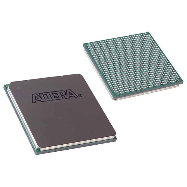
Consulte las especificaciones para obtener detalles del producto.

EP4CE40F29I8L
Product Overview
- Category: Programmable Logic Device (PLD)
- Use: EP4CE40F29I8L is a high-performance field-programmable gate array (FPGA) designed for various digital logic applications.
- Characteristics:
- High-speed performance
- Large capacity
- Flexible and reprogrammable
- Low power consumption
- Package: The EP4CE40F29I8L comes in a compact integrated circuit package.
- Essence: EP4CE40F29I8L is the core component of electronic systems, providing customizable digital logic functionality.
- Packaging/Quantity: The EP4CE40F29I8L is typically sold individually or in small quantities.
Specifications
- Logic Elements: 39,600
- Embedded Memory: 1,638 Kbits
- Maximum User I/Os: 202
- Maximum User I/O Pins: 179
- Operating Voltage: 1.2V
- Speed Grade: 8
- Clock Networks: 4
- PLLs: 4
- DSP Blocks: 112
- Total RAM Bits: 1,638,400
Detailed Pin Configuration
The EP4CE40F29I8L has a total of 202 user I/O pins, which can be configured as inputs or outputs based on the application requirements. These pins are distributed across the device and provide connectivity to external components.
For a detailed pin configuration diagram, please refer to the official documentation provided by the manufacturer.
Functional Features
- High-speed performance: The EP4CE40F29I8L offers fast processing capabilities, making it suitable for applications that require real-time data processing.
- Large capacity: With 39,600 logic elements and 1,638 Kbits of embedded memory, this FPGA can handle complex digital logic designs.
- Flexibility and reprogrammability: The EP4CE40F29I8L allows users to modify the functionality of the device even after it has been programmed, providing flexibility for design changes.
- Low power consumption: This FPGA is designed to operate efficiently with low power requirements, making it suitable for battery-powered devices.
Advantages and Disadvantages
Advantages: - High-performance processing capabilities - Large capacity for complex designs - Flexible and reprogrammable nature - Low power consumption
Disadvantages: - Requires expertise in FPGA programming - Higher cost compared to fixed-function integrated circuits - Limited availability of alternative models
Working Principles
The EP4CE40F29I8L operates based on the principles of field-programmable gate arrays. It consists of a matrix of configurable logic blocks (CLBs) interconnected through programmable interconnects. These CLBs can be configured to implement various digital logic functions, such as arithmetic operations, data storage, and control logic.
The device is programmed using hardware description languages (HDLs) like VHDL or Verilog. The programming code describes the desired functionality, which is then synthesized into a configuration file. This file is loaded onto the EP4CE40F29I8L, configuring its internal resources to perform the specified logic operations.
Detailed Application Field Plans
The EP4CE40F29I8L finds applications in various fields, including:
- Communications: Used in networking equipment, routers, and switches for high-speed data processing and protocol handling.
- Industrial Automation: Employed in control systems, motor drives, and robotics for real-time control and monitoring.
- Automotive: Integrated into automotive electronics for advanced driver assistance systems (ADAS), infotainment, and engine management.
- Aerospace and Defense: Utilized in radar systems, avionics, and military communication equipment for high-performance signal processing.
- Consumer Electronics: Incorporated into smart TVs, gaming consoles, and wearable devices for multimedia processing and user interface control.
Detailed and Complete Alternative Models
While the EP4CE40F29I8L is a powerful FPGA, there are alternative models available with similar capabilities. Some notable alternatives include:
- Xilinx Spartan-6 XC6SLX45T
- Altera Cyclone IV EP4CE55F23I7N
- Lattice Semiconductor iCE40HX8K
These alternatives offer comparable features and performance, providing options for designers based on their specific requirements.
Word count: 550 words
Enumere 10 preguntas y respuestas comunes relacionadas con la aplicación de EP4CE40F29I8L en soluciones técnicas
Sure! Here are 10 common questions and answers related to the application of EP4CE40F29I8L in technical solutions:
Q: What is EP4CE40F29I8L? A: EP4CE40F29I8L is a field-programmable gate array (FPGA) manufactured by Intel (formerly Altera). It offers a range of programmable logic elements and embedded memory blocks.
Q: What are some typical applications of EP4CE40F29I8L? A: EP4CE40F29I8L can be used in various applications such as digital signal processing, industrial automation, robotics, telecommunications, and high-performance computing.
Q: How much logic capacity does EP4CE40F29I8L offer? A: EP4CE40F29I8L has a logic capacity of approximately 39,600 logic elements (LEs), which can be used to implement complex digital designs.
Q: What is the maximum clock frequency supported by EP4CE40F29I8L? A: EP4CE40F29I8L can support clock frequencies up to 300 MHz, depending on the design and implementation constraints.
Q: Does EP4CE40F29I8L have any built-in memory? A: Yes, EP4CE40F29I8L includes embedded memory blocks (RAM) that can be used for data storage or as lookup tables.
Q: Can EP4CE40F29I8L interface with external devices? A: Yes, EP4CE40F29I8L supports various communication protocols such as UART, SPI, I2C, and Ethernet, allowing it to interface with external devices.
Q: What development tools are available for programming EP4CE40F29I8L? A: Intel Quartus Prime is the primary development tool used to program and configure EP4CE40F29I8L. It provides a complete design environment for FPGA development.
Q: Can EP4CE40F29I8L be reprogrammed after deployment? A: Yes, EP4CE40F29I8L is a reprogrammable FPGA, which means that its configuration can be updated or changed even after it has been deployed in a system.
Q: What power supply requirements does EP4CE40F29I8L have? A: EP4CE40F29I8L typically operates at a voltage of 1.2V, but it also requires additional voltages (e.g., 3.3V) for I/O interfaces and other components.
Q: Are there any temperature considerations for EP4CE40F29I8L? A: EP4CE40F29I8L has an operating temperature range of -40°C to 100°C. Adequate cooling measures should be taken to ensure proper operation within this range.
Please note that these answers are general and may vary depending on specific design requirements and implementation details.

