

Consulte las especificaciones para obtener detalles del producto.
EP4SGX110HF35C3N
Product Overview
- Category: Field Programmable Gate Array (FPGA)
- Use: EP4SGX110HF35C3N is a high-performance FPGA designed for various applications in industries such as telecommunications, automotive, aerospace, and consumer electronics.
- Characteristics: This FPGA offers advanced features including high-speed performance, low power consumption, and reconfigurability. It provides a flexible platform for implementing complex digital logic circuits.
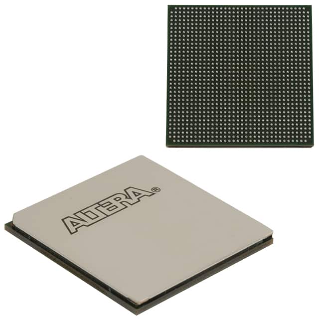
- Package: EP4SGX110HF35C3N comes in a compact package that ensures easy integration into electronic systems.
- Essence: The essence of EP4SGX110HF35C3N lies in its ability to provide customizable hardware solutions for diverse applications.
- Packaging/Quantity: EP4SGX110HF35C3N is typically packaged individually and is available in various quantities depending on the customer's requirements.
Specifications
- Logic Elements: EP4SGX110HF35C3N consists of 110,000 logic elements, allowing for the implementation of complex digital designs.
- Embedded Memory: It includes 4,608 embedded memory blocks, providing ample storage capacity for data processing.
- I/O Pins: EP4SGX110HF35C3N offers 622 I/O pins, enabling seamless communication with external devices.
- Clock Management: It features advanced clock management circuitry, supporting precise timing control.
- Operating Voltage: The FPGA operates at a voltage range of 1.2V to 1.5V, ensuring efficient power utilization.
Detailed Pin Configuration
The pin configuration of EP4SGX110HF35C3N is as follows:
- Pin 1: VCCIO
- Pin 2: GND
- Pin 3: CLK_IN
- Pin 4: RESET
- Pin 5: DATA_IN
- Pin 6: DATA_OUT
- Pin 7: CLK_OUT
- Pin 8: VCCINT
- Pin 9: GND
(Note: This is a simplified representation. The actual pin configuration may include numerous pins for various functionalities.)
Functional Features
- High-Speed Performance: EP4SGX110HF35C3N offers exceptional performance, allowing for rapid data processing and complex computations.
- Reconfigurability: It can be reprogrammed to adapt to changing requirements, providing flexibility in system design.
- Low Power Consumption: The FPGA is designed to minimize power consumption, making it suitable for battery-powered devices.
- Versatile I/O Interface: EP4SGX110HF35C3N supports a wide range of communication protocols, facilitating seamless integration with external devices.
Advantages and Disadvantages
Advantages: - High-performance capabilities - Reconfigurable nature - Low power consumption - Versatile I/O interface
Disadvantages: - Complexity in programming and design implementation - Higher cost compared to traditional fixed-function integrated circuits
Working Principles
EP4SGX110HF35C3N operates based on the principles of field programmable gate arrays. It consists of configurable logic blocks (CLBs), interconnects, embedded memory blocks, and other essential components. The FPGA can be programmed using hardware description languages (HDLs) such as VHDL or Verilog. Once programmed, the FPGA executes the desired digital logic functions by routing signals through the configurable interconnects and CLBs.
Detailed Application Field Plans
EP4SGX110HF35C3N finds applications in various fields, including:
- Telecommunications: Used in high-speed data transmission systems, network routers, and switches.
- Automotive: Employed in advanced driver assistance systems (ADAS), engine control units (ECUs), and infotainment systems.
- Aerospace: Utilized in satellite communication systems, avionics, and flight control systems.
- Consumer Electronics: Integrated into high-definition televisions, gaming consoles, and multimedia devices.
Detailed and Complete Alternative Models
- EP4SGX180HF35C3N: A higher-capacity FPGA with 180,000 logic elements for more complex designs.
- EP4SGX230HF35C3N: Offers even greater logic element capacity (230,000) for demanding applications.
- EP4SGX60HF35C3N: A lower-cost option with 60,000 logic elements suitable for less resource-intensive projects.
(Note: The above alternative models are just a few examples. There are numerous other FPGA models available in the market with varying specifications and capabilities.)
This encyclopedia entry provides an overview of EP4SGX110HF35C3N, including its product details, specifications, pin configuration, functional features, advantages and disadvantages, working principles, application field plans, and alternative models.
Enumere 10 preguntas y respuestas comunes relacionadas con la aplicación de EP4SGX110HF35C3N en soluciones técnicas
Sure! Here are 10 common questions and answers related to the application of EP4SGX110HF35C3N in technical solutions:
1. What is EP4SGX110HF35C3N? EP4SGX110HF35C3N is a high-performance field-programmable gate array (FPGA) manufactured by Intel. It offers a wide range of features and capabilities for implementing complex digital designs.
2. What are the key features of EP4SGX110HF35C3N? Some key features of EP4SGX110HF35C3N include a large number of logic elements, high-speed transceivers, embedded memory blocks, DSP blocks, and support for various I/O standards.
3. What are the typical applications of EP4SGX110HF35C3N? EP4SGX110HF35C3N is commonly used in applications such as telecommunications, networking equipment, high-performance computing, video processing, and industrial automation.
4. How can EP4SGX110HF35C3N be programmed? EP4SGX110HF35C3N can be programmed using hardware description languages (HDLs) such as VHDL or Verilog. Designers can write code to describe the desired functionality and then use software tools provided by Intel to compile and program the FPGA.
5. Can EP4SGX110HF35C3N be reprogrammed? Yes, EP4SGX110HF35C3N is a reprogrammable FPGA. This means that after programming, if there is a need to change the design or functionality, the FPGA can be reprogrammed with a new configuration.
6. What is the maximum operating frequency of EP4SGX110HF35C3N? The maximum operating frequency of EP4SGX110HF35C3N depends on the design and implementation. However, it is capable of operating at high frequencies, typically in the range of several hundred megahertz to a few gigahertz.
7. Does EP4SGX110HF35C3N support high-speed serial communication? Yes, EP4SGX110HF35C3N has built-in high-speed transceivers that support various protocols such as PCIe, Ethernet, SATA, and USB. These transceivers enable high-speed serial communication between the FPGA and external devices.
8. Can EP4SGX110HF35C3N interface with other components or devices? Yes, EP4SGX110HF35C3N supports various I/O standards and can interface with other components or devices such as memories, sensors, displays, and communication interfaces. It provides flexible I/O options to accommodate different requirements.
9. What are the power requirements for EP4SGX110HF35C3N? EP4SGX110HF35C3N requires a supply voltage of 1.2V for core logic and 3.3V for I/O banks. The power consumption depends on the design and utilization of the FPGA resources.
10. Are there any development boards or evaluation kits available for EP4SGX110HF35C3N? Yes, Intel provides development boards and evaluation kits specifically designed for EP4SGX110HF35C3N. These boards come with necessary hardware interfaces, software tools, and documentation to aid in the development and testing of FPGA designs.
Please note that the specific details and answers may vary depending on the context and requirements of the technical solution.