

Consulte las especificaciones para obtener detalles del producto.
LC4128B-27TN128C
Product Overview
Category
LC4128B-27TN128C belongs to the category of programmable logic devices (PLDs).
Use
It is primarily used for digital circuit design and implementation.
Characteristics
- Programmable: LC4128B-27TN128C can be programmed to perform specific functions.
- High-speed operation: It operates at a clock frequency of 27 MHz, enabling fast processing.
- Non-volatile: The device retains its programmed configuration even when power is removed.
- Low power consumption: LC4128B-27TN128C is designed to consume minimal power during operation.
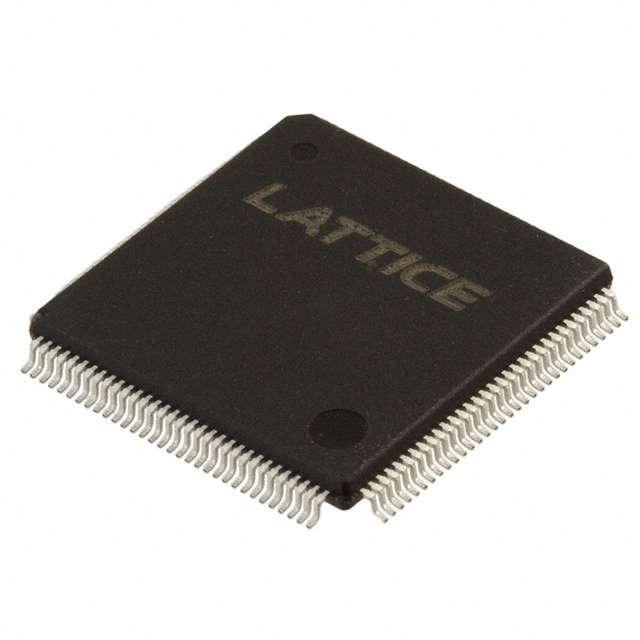
Package
The LC4128B-27TN128C comes in a compact package that ensures easy integration into electronic circuits.
Essence
The essence of LC4128B-27TN128C lies in its ability to provide flexible and customizable digital circuit solutions.
Packaging/Quantity
The device is typically packaged in trays or tubes, with each containing a specified quantity of LC4128B-27TN128C units.
Specifications
- Operating Frequency: 27 MHz
- Logic Cells: 128
- I/O Pins: 28
- Supply Voltage: 3.3V
- Operating Temperature Range: -40°C to 85°C
Detailed Pin Configuration
The LC4128B-27TN128C has a total of 28 pins, each serving a specific purpose in the device's functionality. A detailed pin configuration diagram can be found in the product datasheet.
Functional Features
- Flexible Logic Design: LC4128B-27TN128C allows users to implement various logic functions based on their requirements.
- In-system Programming: The device supports in-system programming, enabling easy updates and modifications.
- JTAG Boundary Scan: It features JTAG boundary scan capability, facilitating efficient testing and debugging.
Advantages and Disadvantages
Advantages
- Versatility: LC4128B-27TN128C can be programmed to perform a wide range of functions, making it suitable for diverse applications.
- Cost-effective: The device offers cost advantages compared to traditional discrete logic components.
- Compact Size: Its small form factor allows for space-efficient integration into electronic systems.
Disadvantages
- Limited Capacity: With 128 logic cells, LC4128B-27TN128C may not be suitable for complex designs requiring a higher number of logic elements.
- Programming Complexity: Programming the device requires knowledge of hardware description languages and PLD programming techniques.
Working Principles
LC4128B-27TN128C operates based on the principles of programmable logic. It consists of configurable logic blocks (CLBs), interconnect resources, and input/output blocks (IOBs). The CLBs can be programmed to implement various logic functions, while the interconnect resources facilitate the routing of signals between different CLBs. The IOBs provide the interface between the device and external circuitry.
Detailed Application Field Plans
LC4128B-27TN128C finds applications in various fields, including but not limited to: - Industrial automation - Consumer electronics - Telecommunications - Automotive systems - Medical devices
In industrial automation, it can be used for control systems and process monitoring. In consumer electronics, it can enable the implementation of custom digital functions. Telecommunications applications may include signal processing and protocol handling. LC4128B-27TN128C can also be utilized in automotive systems for control and monitoring purposes. Additionally, it can be integrated into medical devices for data acquisition and processing.
Detailed and Complete Alternative Models
There are several alternative models available in the market that offer similar functionality to LC4128B-27TN128C. Some notable alternatives include: - Xilinx Spartan-6 FPGA - Altera Cyclone IV E FPGA - Lattice iCE40 FPGA
These alternative models provide varying capacities, features, and price points, allowing users to choose the most suitable option for their specific requirements.
Word count: 518
Enumere 10 preguntas y respuestas comunes relacionadas con la aplicación de LC4128B-27TN128C en soluciones técnicas
Sure! Here are 10 common questions and answers related to the application of LC4128B-27TN128C in technical solutions:
Q: What is LC4128B-27TN128C? A: LC4128B-27TN128C is a specific model of a low-power, high-density programmable logic device (PLD) manufactured by Lattice Semiconductor.
Q: What are the key features of LC4128B-27TN128C? A: LC4128B-27TN128C offers 128 macrocells, operates at a speed grade of 27ns, has a total of 128 inputs/outputs (I/Os), and supports various I/O standards.
Q: What are some typical applications of LC4128B-27TN128C? A: LC4128B-27TN128C can be used in a wide range of applications, including industrial control systems, automotive electronics, telecommunications equipment, and consumer electronics.
Q: How does LC4128B-27TN128C compare to other PLDs on the market? A: LC4128B-27TN128C offers a good balance between performance, power consumption, and cost, making it suitable for many general-purpose applications.
Q: Can LC4128B-27TN128C be reprogrammed after it has been configured? A: No, LC4128B-27TN128C is a one-time programmable (OTP) device, meaning that its configuration cannot be changed once programmed.
Q: What development tools are available for designing with LC4128B-27TN128C? A: Lattice Semiconductor provides software tools like Lattice Diamond or iCEcube2, which offer design entry, synthesis, simulation, and programming capabilities.
Q: What voltage levels does LC4128B-27TN128C support? A: LC4128B-27TN128C supports both 3.3V and 5V I/O standards, making it compatible with a wide range of digital systems.
Q: Can LC4128B-27TN128C interface with other devices or microcontrollers? A: Yes, LC4128B-27TN128C can interface with other devices using standard protocols like SPI, I2C, UART, or GPIOs.
Q: Are there any limitations to the number of inputs/outputs that LC4128B-27TN128C can handle? A: LC4128B-27TN128C has a total of 128 I/O pins, but the actual number of usable I/Os may vary depending on the specific configuration and design requirements.
Q: Where can I find more information about LC4128B-27TN128C and its application notes? A: Lattice Semiconductor's website provides detailed documentation, datasheets, application notes, and reference designs for LC4128B-27TN128C, which can be accessed for further information.
Please note that the answers provided here are general and may vary based on specific requirements and use cases. It is always recommended to refer to the official documentation and consult with technical experts for accurate and up-to-date information.