Consulte las especificaciones para obtener detalles del producto.

LC4128ZC-42TN100C
Product Overview
Category: Integrated Circuit (IC)
Use: LC4128ZC-42TN100C is a programmable logic device (PLD) that belongs to the family of Complex Programmable Logic Devices (CPLDs). It is designed for digital logic applications and offers high-performance capabilities.
Characteristics: - High-density programmable logic device - Low power consumption - Fast propagation delay - Flexible design options - Easy integration with other components
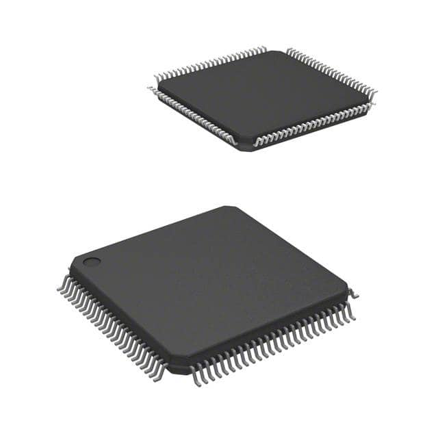
Package: The LC4128ZC-42TN100C is available in a 100-pin Thin Quad Flat Pack (TQFP) package. This package provides a compact form factor and allows for easy mounting on circuit boards.
Essence: The essence of LC4128ZC-42TN100C lies in its ability to provide designers with a versatile and efficient solution for implementing complex digital logic functions.
Packaging/Quantity: The LC4128ZC-42TN100C is typically sold in reels or trays, with a quantity of 250 units per reel/tray.
Specifications
- Number of Logic Cells: 128
- Maximum Operating Frequency: 42 MHz
- Number of I/O Pins: 100
- Supply Voltage: 3.3V
- Operating Temperature Range: -40°C to +85°C
- Programmable Logic Blocks: 32
- Macrocells: 128
- On-Chip Memory: 2,048 bits
Pin Configuration
The LC4128ZC-42TN100C has a total of 100 pins, which are assigned different functions based on their configuration. Here is a brief overview of the pinout:
- VCCIO: Power supply pin for I/O buffers
- GND: Ground pin
- TCK/TMS/TDI/TDO: JTAG interface pins for programming and debugging
- I/O Pins: General-purpose input/output pins for connecting to external devices
- Clock Inputs: Pins for providing clock signals to the device
- Configuration Pins: Pins for configuring the device during startup
For a detailed pin configuration diagram, please refer to the datasheet provided by the manufacturer.
Functional Features
The LC4128ZC-42TN100C offers several functional features that make it suitable for a wide range of applications:
Programmability: The device can be programmed to implement various digital logic functions, allowing designers to customize its behavior according to their specific requirements.
High-Speed Operation: With a maximum operating frequency of 42 MHz, the LC4128ZC-42TN100C can handle complex logic operations with minimal delay.
Flexible I/O Options: The device provides a generous number of I/O pins, enabling seamless integration with other components and peripherals.
Low Power Consumption: The LC4128ZC-42TN100C is designed to operate efficiently, consuming minimal power while delivering high-performance results.
Advantages and Disadvantages
Advantages: - High-density programmable logic device - Versatile and flexible design options - Fast propagation delay - Low power consumption - Easy integration with other components
Disadvantages: - Limited number of logic cells compared to larger CPLDs - Relatively smaller on-chip memory capacity
Working Principles
The LC4128ZC-42TN100C operates based on the principles of programmable logic. It consists of configurable logic blocks (CLBs) that contain look-up tables (LUTs), flip-flops, and other essential elements. These CLBs are interconnected through programmable interconnect resources, allowing designers to create complex logic circuits.
During operation, the device is programmed using a hardware description language (HDL) or a schematic entry tool. The programming configures the CLBs and interconnect resources to implement the desired logic functions. Once programmed, the device can perform the specified operations based on the applied inputs.
Detailed Application Field Plans
The LC4128ZC-42TN100C finds applications in various fields, including:
Embedded Systems: It can be used in embedded systems for controlling and managing peripheral devices, such as sensors, actuators, and displays.
Communications: The device can be employed in communication systems for protocol handling, data routing, and signal processing.
Industrial Automation: It is suitable for implementing control logic in industrial automation systems, enabling efficient monitoring and control of manufacturing processes.
Consumer Electronics: The LC4128ZC-42TN100C can be utilized in consumer electronics products, such as gaming consoles, set-top boxes, and home automation systems.
Alternative Models
In addition to the LC4128ZC-42TN100C, there are several alternative models available in the market that offer similar functionality. Some notable
Enumere 10 preguntas y respuestas comunes relacionadas con la aplicación de LC4128ZC-42TN100C en soluciones técnicas
Sure! Here are 10 common questions and answers related to the application of LC4128ZC-42TN100C in technical solutions:
Q: What is LC4128ZC-42TN100C? A: LC4128ZC-42TN100C is a specific model of programmable logic device (PLD) manufactured by Lattice Semiconductor.
Q: What are the key features of LC4128ZC-42TN100C? A: Some key features of LC4128ZC-42TN100C include 128 macrocells, 128 inputs/outputs, 42 MHz maximum operating frequency, and a TQFP-100 package.
Q: What are the typical applications of LC4128ZC-42TN100C? A: LC4128ZC-42TN100C is commonly used in various technical solutions such as industrial automation, consumer electronics, telecommunications, automotive systems, and more.
Q: How does LC4128ZC-42TN100C differ from other PLDs? A: LC4128ZC-42TN100C offers a balance between cost, performance, and power consumption, making it suitable for a wide range of applications. It also has specific features and capabilities unique to its model.
Q: Can LC4128ZC-42TN100C be programmed? A: Yes, LC4128ZC-42TN100C is a programmable logic device, which means it can be configured and programmed to perform specific functions based on the user's requirements.
Q: What programming languages or tools are compatible with LC4128ZC-42TN100C? A: LC4128ZC-42TN100C can be programmed using hardware description languages (HDLs) such as VHDL or Verilog. Lattice Semiconductor provides software tools like Lattice Diamond or iCEcube2 for programming and design implementation.
Q: Can LC4128ZC-42TN100C be used in high-speed applications? A: Yes, LC4128ZC-42TN100C has a maximum operating frequency of 42 MHz, which makes it suitable for many high-speed applications.
Q: Are there any limitations to the number of inputs/outputs in LC4128ZC-42TN100C? A: LC4128ZC-42TN100C has 128 inputs/outputs, which should be sufficient for most applications. However, if more I/Os are required, other PLD models with higher I/O counts can be considered.
Q: Can LC4128ZC-42TN100C interface with other components or devices? A: Yes, LC4128ZC-42TN100C can interface with various components and devices through its I/O pins, allowing communication and integration with other parts of a system.
Q: Where can I find additional technical information about LC4128ZC-42TN100C? A: You can refer to the datasheet and technical documentation provided by Lattice Semiconductor for detailed specifications, application notes, and reference designs related to LC4128ZC-42TN100C.

