

Consulte las especificaciones para obtener detalles del producto.
LC4384V-35T176C
Product Overview
Category: Integrated Circuit (IC)
Use: The LC4384V-35T176C is a programmable logic device (PLD) that belongs to the family of Complex Programmable Logic Devices (CPLDs). It is designed for use in various digital applications where high-performance and flexibility are required.
Characteristics: - High-density programmable logic device - Low power consumption - Fast propagation delay - Large number of input/output pins - Flexible architecture for easy customization
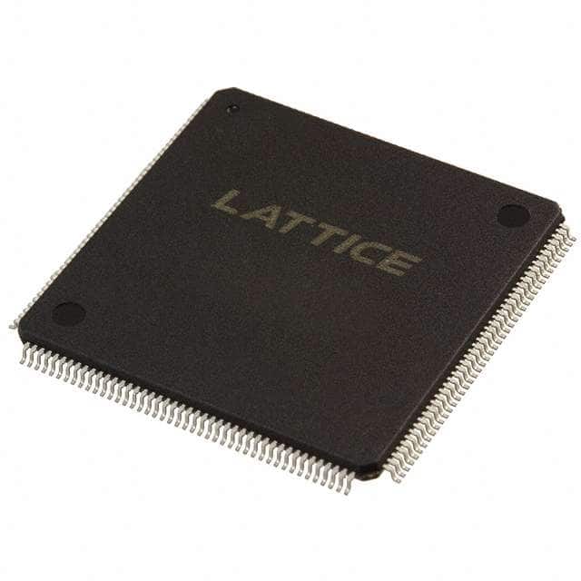
Package: The LC4384V-35T176C is available in a 176-pin Thin Quad Flat Pack (TQFP) package. This package provides good thermal performance and ease of soldering.
Essence: The essence of the LC4384V-35T176C lies in its ability to provide a highly configurable and versatile solution for digital circuit design. It offers a wide range of features and capabilities that can be tailored to specific application requirements.
Packaging/Quantity: The LC4384V-35T176C is typically sold in reels or trays, with a quantity of 250 units per reel/tray.
Specifications
- Maximum Operating Frequency: 35 MHz
- Number of Logic Cells: 384
- Number of I/O Pins: 176
- Supply Voltage: 3.3V
- Operating Temperature Range: -40°C to +85°C
Pin Configuration
The LC4384V-35T176C has a total of 176 pins, which are divided into different categories:
- Power Supply Pins (VCC, GND)
- Input/Output Pins (I/O)
- Clock Pins (CLK)
- Configuration Pins (CFG)
- Control Pins (CTL)
- Reset Pins (RST)
- Test Pins (TEST)
For a detailed pin configuration diagram, please refer to the datasheet provided by the manufacturer.
Functional Features
- High-speed programmable logic device with low power consumption
- Flexible architecture allows for easy customization and design modifications
- Supports various I/O standards and interfaces
- On-chip memory elements for efficient data storage and retrieval
- Built-in clock management circuitry for precise timing control
- JTAG interface for programming and debugging capabilities
Advantages and Disadvantages
Advantages: - High-density integration enables complex digital designs - Low power consumption extends battery life in portable applications - Fast propagation delay ensures high-speed operation - Flexible architecture allows for easy design modifications - Wide range of I/O pins provides versatility in interfacing with other devices
Disadvantages: - Limited maximum operating frequency compared to some other programmable logic devices - Relatively higher cost compared to simpler logic devices - Steeper learning curve for beginners due to its complexity
Working Principles
The LC4384V-35T176C operates based on the principles of programmable logic. It consists of an array of configurable logic blocks interconnected through programmable interconnects. These logic blocks can be programmed to implement various digital functions such as combinatorial logic, sequential logic, and memory elements.
The device is configured using a hardware description language (HDL) or a schematic entry tool. The configuration data is then loaded into the device's internal memory through a programming interface. Once configured, the device performs the desired digital functions based on the programmed logic.
Detailed Application Field Plans
The LC4384V-35T176C finds applications in various fields where flexible and high-performance digital circuitry is required. Some of the common application areas include:
- Communication Systems: Used for protocol conversion, signal processing, and interface control in communication systems.
- Industrial Automation: Employed in control systems, motor drives, and process automation for efficient and reliable operation.
- Consumer Electronics: Integrated into devices such as gaming consoles, set-top boxes, and multimedia players for enhanced functionality.
- Automotive Electronics: Utilized in automotive control units, infotainment systems, and driver assistance systems for improved performance and safety.
- Medical Devices: Incorporated into medical equipment for data acquisition, signal processing, and control functions.
Detailed and Complete Alternative Models
- LC4128V-75T100C: A lower-density CPLD with 128 logic cells and 100 I/O pins. Suitable for applications with less complex digital designs.
- LC4064V-75TN44C: A smaller package variant of the LC4384V-35T176C with 64 logic cells and 44 I/O pins. Ideal for space-constrained designs.
- LC4512V-120T176I: A higher-density CPLD with 512 logic cells and 176 I/O pins. Offers increased capacity for more complex digital designs.
These alternative models provide options with varying densities and pin counts
Enumere 10 preguntas y respuestas comunes relacionadas con la aplicación de LC4384V-35T176C en soluciones técnicas
Sure! Here are 10 common questions and answers related to the application of LC4384V-35T176C in technical solutions:
1. What is LC4384V-35T176C? LC4384V-35T176C is a specific model of Field Programmable Gate Array (FPGA) manufactured by Lattice Semiconductor. It offers 3840 Look-Up Tables (LUTs), 64Kbits of embedded block RAM, and operates at a speed grade of 35.
2. What are the typical applications of LC4384V-35T176C? LC4384V-35T176C is commonly used in various technical solutions such as industrial automation, telecommunications, automotive electronics, medical devices, and consumer electronics.
3. What are the key features of LC4384V-35T176C? Some key features of LC4384V-35T176C include low power consumption, high-performance architecture, on-chip memory blocks, programmable I/O pins, and support for various communication protocols.
4. How can LC4384V-35T176C be programmed? LC4384V-35T176C can be programmed using Hardware Description Languages (HDLs) like VHDL or Verilog. Designers can write code to describe the desired functionality and then use synthesis tools to convert it into a configuration file that can be loaded onto the FPGA.
5. Can LC4384V-35T176C be reprogrammed? Yes, LC4384V-35T176C is a reprogrammable FPGA. It can be reconfigured multiple times to implement different designs or to make changes to the existing design.
6. What development tools are available for working with LC4384V-35T176C? Lattice Semiconductor provides development tools like Lattice Diamond, Lattice Radiant, and Lattice iCEcube2 for designing, simulating, and programming LC4384V-35T176C.
7. What is the maximum operating frequency of LC4384V-35T176C? The maximum operating frequency of LC4384V-35T176C depends on the design and implementation. However, it is typically capable of operating at frequencies up to 100 MHz or higher.
8. Can LC4384V-35T176C interface with other components or devices? Yes, LC4384V-35T176C supports various communication protocols like SPI, I2C, UART, and GPIOs, allowing it to interface with other components or devices in a system.
9. Are there any limitations or considerations when using LC4384V-35T176C? Some considerations include power supply requirements, thermal management, signal integrity, and the need for external components like voltage regulators or clock sources.
10. Where can I find more information about LC4384V-35T176C? You can find more detailed information about LC4384V-35T176C, including datasheets, application notes, and reference designs, on the official website of Lattice Semiconductor or by contacting their technical support team.