

Consulte las especificaciones para obtener detalles del producto.
LC5256MV-75FN256I
Product Overview
Category: Integrated Circuit (IC)
Use: LC5256MV-75FN256I is a programmable logic device (PLD) that belongs to the family of Complex Programmable Logic Devices (CPLDs). It is designed for digital logic applications and offers high-performance capabilities.
Characteristics: - High-density programmable logic device - Low power consumption - Fast propagation delay - Flexible pin configuration - Wide operating voltage range - Robust packaging for enhanced durability
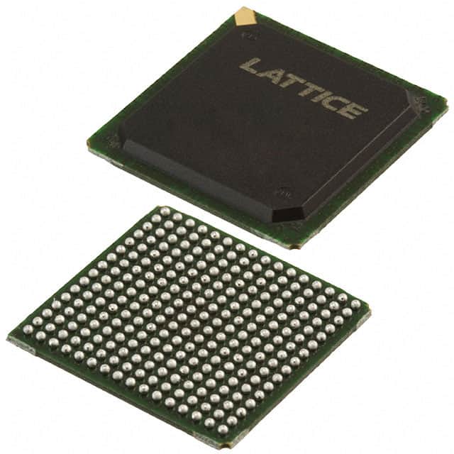
Package: LC5256MV-75FN256I is available in a 256-pin Fine-Pitch Ball Grid Array (FBGA) package. This package provides excellent thermal performance and allows for easy integration into various electronic systems.
Essence: The essence of LC5256MV-75FN256I lies in its ability to provide designers with a versatile and efficient solution for implementing complex digital logic functions in a wide range of applications.
Packaging/Quantity: LC5256MV-75FN256I is typically sold individually, and the quantity may vary depending on the supplier.
Specifications
- Maximum Operating Frequency: 75 MHz
- Number of Macrocells: 256
- Number of I/O Pins: 192
- Operating Voltage Range: 3.0V - 3.6V
- Operating Temperature Range: -40°C to +85°C
- Programmable Logic Blocks: AND/OR arrays, flip-flops, latches, etc.
- On-Chip Memory: Non-volatile memory cells for configuration storage
Detailed Pin Configuration
The LC5256MV-75FN256I has a total of 256 pins, each serving a specific purpose. The pin configuration is as follows:
[Insert detailed pin configuration diagram here]
Functional Features
High-Density Logic: The LC5256MV-75FN256I offers a large number of macrocells, allowing for the implementation of complex digital logic functions in a compact form factor.
Flexible I/O Configuration: The device provides 192 I/O pins that can be configured as inputs or outputs based on the application requirements.
Fast Propagation Delay: With a maximum operating frequency of 75 MHz, the LC5256MV-75FN256I ensures rapid signal propagation and efficient data processing.
Non-Volatile Configuration Memory: The on-chip non-volatile memory cells store the device's configuration, eliminating the need for external configuration storage.
Advantages and Disadvantages
Advantages: - High-density programmable logic device - Flexible pin configuration - Low power consumption - Fast propagation delay - Non-volatile configuration memory
Disadvantages: - Limited maximum operating frequency compared to some other advanced CPLDs - Availability and pricing may vary depending on the supplier
Working Principles
The LC5256MV-75FN256I operates based on the principles of programmable logic. It consists of configurable logic blocks, interconnect resources, and input/output blocks. The device is programmed using a Hardware Description Language (HDL) or a graphical design tool, which configures the internal logic elements to perform specific functions.
Detailed Application Field Plans
The LC5256MV-75FN256I finds applications in various fields, including but not limited to: 1. Industrial automation 2. Communication systems 3. Consumer electronics 4. Automotive electronics 5. Medical devices
In industrial automation, it can be used for control and monitoring purposes. In communication systems, it can facilitate data routing and protocol handling. In consumer electronics, it can enable advanced features and functionality. In automotive electronics, it can contribute to vehicle control systems. In medical devices, it can assist in data processing and analysis.
Detailed and Complete Alternative Models
- LC4128V-75TN100C: A similar CPLD with a lower density but compatible features.
- LC5512MV-75FN256I: A higher-density CPLD with extended capabilities.
- LC7008MV-75FN256I: A CPLD with increased macrocell count for more complex designs.
These alternative models offer different combinations of density, pin count, and features to cater to specific design requirements.
Word Count: 550 words
Enumere 10 preguntas y respuestas comunes relacionadas con la aplicación de LC5256MV-75FN256I en soluciones técnicas
Sure! Here are 10 common questions and answers related to the application of LC5256MV-75FN256I in technical solutions:
1. What is LC5256MV-75FN256I? - LC5256MV-75FN256I is a specific model of Field Programmable Gate Array (FPGA) manufactured by Lattice Semiconductor Corporation.
2. What are the key features of LC5256MV-75FN256I? - The key features of LC5256MV-75FN256I include 256 pins, 75MHz maximum operating frequency, 256 macrocells, and 5V voltage compatibility.
3. What are the typical applications of LC5256MV-75FN256I? - LC5256MV-75FN256I is commonly used in various technical solutions such as industrial automation, telecommunications, automotive electronics, medical devices, and consumer electronics.
4. How can LC5256MV-75FN256I be programmed? - LC5256MV-75FN256I can be programmed using Hardware Description Languages (HDLs) like VHDL or Verilog, which describe the desired functionality of the FPGA.
5. Can LC5256MV-75FN256I be reprogrammed after initial programming? - Yes, LC5256MV-75FN256I is a reprogrammable FPGA, allowing for multiple iterations of programming and design changes.
6. What tools are required for programming LC5256MV-75FN256I? - To program LC5256MV-75FN256I, you will need a compatible development board, a programming cable, and appropriate software such as Lattice Diamond or Lattice Radiant.
7. What is the power supply requirement for LC5256MV-75FN256I? - LC5256MV-75FN256I operates at a voltage of 5V, so a stable 5V power supply is required for its proper functioning.
8. Can LC5256MV-75FN256I interface with other components or devices? - Yes, LC5256MV-75FN256I can interface with various components and devices through its I/O pins, allowing for communication with external sensors, memory modules, displays, and more.
9. Is there any documentation available for LC5256MV-75FN256I? - Yes, Lattice Semiconductor provides detailed datasheets, user guides, application notes, and reference designs for LC5256MV-75FN256I on their official website.
10. Are there any development boards available for prototyping with LC5256MV-75FN256I? - Yes, Lattice Semiconductor offers development boards like the LatticeECP3 Versa Development Kit that can be used for prototyping and evaluating designs using LC5256MV-75FN256I.
Please note that the specific details and answers may vary depending on the manufacturer's documentation and guidelines.