

Consulte las especificaciones para obtener detalles del producto.
LCMXO2-1200ZE-3MG132C
Product Overview
Category
The LCMXO2-1200ZE-3MG132C belongs to the category of Field Programmable Gate Arrays (FPGAs).
Use
FPGAs are integrated circuits that can be programmed after manufacturing. The LCMXO2-1200ZE-3MG132C is specifically designed for digital logic applications.
Characteristics
- Low power consumption
- High performance
- Small form factor
- Flexible and reconfigurable
Package
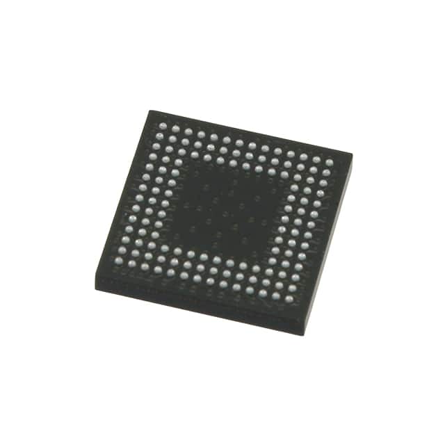
The LCMXO2-1200ZE-3MG132C comes in a 132-pin Quad Flat No-Lead (QFN) package.
Essence
The essence of the LCMXO2-1200ZE-3MG132C lies in its ability to provide a customizable hardware solution for various digital logic applications.
Packaging/Quantity
The LCMXO2-1200ZE-3MG132C is typically sold individually, and the quantity may vary depending on the supplier.
Specifications
- FPGA Family: Lattice XO2
- Logic Elements: 1200
- Macrocells: 1280
- Operating Voltage: 1.2V
- Speed Grade: -3
- I/O Pins: 132
- Maximum Frequency: 100 MHz
- Configuration Memory: 256 kbits
- Embedded Block RAM: 64 kbits
- PLLs: 2
Detailed Pin Configuration
The LCMXO2-1200ZE-3MG132C has a total of 132 pins. The pin configuration is as follows:
- Pin 1: VCCIO
- Pin 2: GND
- Pin 3: IOL1PCCLK_0
- Pin 4: IOL1NCCLK_0
- Pin 5: IOL2PCCLK_0
- ...
- Pin 132: GND
Functional Features
- Reconfigurable logic elements for implementing custom digital circuits
- Embedded memory blocks for data storage
- Dedicated input/output pins for interfacing with external devices
- Clock management resources for precise timing control
- Support for various communication protocols
Advantages and Disadvantages
Advantages
- Flexibility to adapt to changing requirements
- Lower development time compared to custom ASICs
- Cost-effective for low to medium volume production
- Ability to prototype and test designs before committing to manufacturing
Disadvantages
- Limited performance compared to dedicated hardware solutions
- Higher power consumption compared to application-specific integrated circuits (ASICs)
- Complexity in programming and configuring the FPGA
Working Principles
The LCMXO2-1200ZE-3MG132C works based on the principle of reconfigurable logic. It consists of a matrix of programmable logic elements that can be interconnected to implement desired digital circuits. The configuration of these logic elements is stored in non-volatile memory, allowing the FPGA to retain its programmed functionality even after power cycles.
Detailed Application Field Plans
The LCMXO2-1200ZE-3MG132C finds applications in various fields, including:
- Embedded Systems: Used for implementing custom logic in microcontroller-based systems.
- Communications: Employed in networking equipment for protocol handling and data processing.
- Industrial Automation: Utilized for control and monitoring tasks in industrial machinery.
- Signal Processing: Applied in audio and video processing systems for real-time data manipulation.
- Test and Measurement: Used in test equipment for signal generation, analysis, and protocol emulation.
Detailed and Complete Alternative Models
- Xilinx Spartan-6 XC6SLX9
- Altera Cyclone IV EP4CE6
- Microsemi IGLOO2 M2GL090
These alternative models offer similar functionality and can be considered as alternatives to the LCMXO2-1200ZE-3MG132C.
Word count: 529 words
Enumere 10 preguntas y respuestas comunes relacionadas con la aplicación de LCMXO2-1200ZE-3MG132C en soluciones técnicas
Sure! Here are 10 common questions and answers related to the application of LCMXO2-1200ZE-3MG132C in technical solutions:
Q: What is the LCMXO2-1200ZE-3MG132C? A: The LCMXO2-1200ZE-3MG132C is a low-cost, low-power FPGA (Field-Programmable Gate Array) device manufactured by Lattice Semiconductor.
Q: What are the key features of the LCMXO2-1200ZE-3MG132C? A: Some key features include 1200 Look-Up Tables (LUTs), 64 Kbits of embedded block RAM, 49 user I/O pins, and support for various I/O standards.
Q: What are some typical applications of the LCMXO2-1200ZE-3MG132C? A: The LCMXO2-1200ZE-3MG132C is commonly used in applications such as industrial control systems, consumer electronics, medical devices, and communication equipment.
Q: How can I program the LCMXO2-1200ZE-3MG132C? A: The LCMXO2-1200ZE-3MG132C can be programmed using Lattice Diamond or Lattice Radiant software tools, which provide a graphical interface for designing and programming the FPGA.
Q: What is the power consumption of the LCMXO2-1200ZE-3MG132C? A: The LCMXO2-1200ZE-3MG132C has low power consumption, typically ranging from 25mW to 150mW, depending on the design and operating conditions.
Q: Can I use the LCMXO2-1200ZE-3MG132C in battery-powered devices? A: Yes, the low power consumption of the LCMXO2-1200ZE-3MG132C makes it suitable for battery-powered applications where power efficiency is crucial.
Q: Does the LCMXO2-1200ZE-3MG132C support communication interfaces? A: Yes, the LCMXO2-1200ZE-3MG132C supports various communication interfaces such as SPI, I2C, UART, and GPIO, making it versatile for different applications.
Q: Can I use the LCMXO2-1200ZE-3MG132C for real-time signal processing? A: Yes, the LCMXO2-1200ZE-3MG132C's high-speed performance and embedded block RAM make it suitable for real-time signal processing applications.
Q: Is the LCMXO2-1200ZE-3MG132C compatible with other FPGA devices? A: The LCMXO2-1200ZE-3MG132C follows the Lattice Semiconductor's ispLEVER Classic design flow, which allows compatibility with other Lattice FPGA devices.
Q: Where can I find technical documentation and support for the LCMXO2-1200ZE-3MG132C? A: You can find technical documentation, datasheets, application notes, and support resources on the official Lattice Semiconductor website or by contacting their customer support team.
Please note that the answers provided here are general and may vary depending on specific requirements and use cases.