

Consulte las especificaciones para obtener detalles del producto.
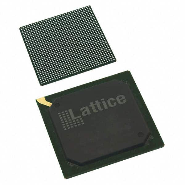
LFE3-70EA-9FN1156C
Product Overview
Category
The LFE3-70EA-9FN1156C belongs to the category of Field Programmable Gate Arrays (FPGAs).
Use
This FPGA is primarily used in electronic circuits for digital logic implementation, prototyping, and system integration.
Characteristics
- High-performance programmable logic device
- Offers flexibility and reconfigurability
- Enables rapid development and customization of digital systems
- Supports complex designs and algorithms
- Provides high-speed data processing capabilities
Package
The LFE3-70EA-9FN1156C comes in a compact and durable package, ensuring protection during handling and installation.
Essence
The essence of this FPGA lies in its ability to provide a versatile platform for implementing complex digital circuits with high performance and flexibility.
Packaging/Quantity
Each package of LFE3-70EA-9FN1156C contains one unit of the FPGA.
Specifications
- Model: LFE3-70EA-9FN1156C
- Logic Elements: 70,000
- Number of I/O Pins: 1,156
- Operating Voltage: 1.2V
- Maximum Frequency: 500 MHz
- Configuration Memory: 4 Mb
- Embedded Memory: 2,048 Kb
- DSP Blocks: 360
- Package Type: BGA (Ball Grid Array)
- Package Dimensions: 23mm x 23mm
Detailed Pin Configuration
The LFE3-70EA-9FN1156C has a total of 1,156 pins, each serving a specific purpose in the circuit design. The pin configuration includes input/output pins, power supply pins, clock pins, and configuration pins. A detailed pinout diagram can be found in the product datasheet.
Functional Features
- High-speed data processing capabilities
- Reconfigurable logic elements for flexible design implementation
- Embedded memory blocks for efficient storage and retrieval of data
- Dedicated DSP blocks for performing complex mathematical operations
- Support for various communication protocols and interfaces
- Low power consumption for energy-efficient operation
Advantages and Disadvantages
Advantages
- Versatile platform for implementing complex digital circuits
- Rapid development and customization of digital systems
- High-performance capabilities for demanding applications
- Flexibility to adapt to changing design requirements
- Efficient utilization of resources for optimized system performance
Disadvantages
- Steep learning curve for beginners due to the complexity of FPGA programming
- Higher cost compared to traditional fixed-function integrated circuits
- Limited availability of alternative models with similar specifications
Working Principles
The LFE3-70EA-9FN1156C operates based on the principles of reconfigurable computing. It consists of a matrix of programmable logic elements interconnected through configurable routing resources. The device can be programmed to implement desired digital logic functions by configuring the interconnections between logic elements.
Detailed Application Field Plans
The LFE3-70EA-9FN1156C finds extensive application in various fields, including: 1. Telecommunications: Used in network routers, switches, and base stations for high-speed data processing. 2. Aerospace and Defense: Employed in radar systems, avionics, and military communication equipment. 3. Industrial Automation: Integrated into control systems for process automation and monitoring. 4. Medical Electronics: Utilized in medical imaging devices, patient monitoring systems, and diagnostic equipment. 5. Automotive: Incorporated in advanced driver assistance systems (ADAS) and infotainment systems.
Detailed and Complete Alternative Models
While the LFE3-70EA-9FN1156C offers a comprehensive set of features, there are alternative FPGA models available in the market with similar capabilities. Some notable alternatives include: - Xilinx Virtex UltraScale+ FPGA - Intel Stratix 10 FPGA - Microchip PolarFire FPGA - Lattice ECP5 FPGA
These alternative models provide comparable performance and functionality, allowing designers to choose the most suitable FPGA for their specific application requirements.
Word count: 570 words
Enumere 10 preguntas y respuestas comunes relacionadas con la aplicación de LFE3-70EA-9FN1156C en soluciones técnicas
Sure! Here are 10 common questions and answers related to the application of LFE3-70EA-9FN1156C in technical solutions:
Q: What is the LFE3-70EA-9FN1156C? A: The LFE3-70EA-9FN1156C is a specific model of Field-Programmable Gate Array (FPGA) manufactured by Lattice Semiconductor.
Q: What are the key features of the LFE3-70EA-9FN1156C? A: The LFE3-70EA-9FN1156C offers features such as high-performance logic fabric, embedded memory blocks, high-speed I/O interfaces, and low power consumption.
Q: In what applications can the LFE3-70EA-9FN1156C be used? A: The LFE3-70EA-9FN1156C can be used in various applications including telecommunications, industrial automation, automotive electronics, medical devices, and aerospace systems.
Q: What is the maximum number of logic elements available in the LFE3-70EA-9FN1156C? A: The LFE3-70EA-9FN1156C has a maximum of 70,000 logic elements (LEs) that can be utilized for implementing complex digital designs.
Q: Can the LFE3-70EA-9FN1156C support high-speed serial communication protocols? A: Yes, the LFE3-70EA-9FN1156C supports high-speed serial communication protocols such as PCIe, Gigabit Ethernet, USB, and SATA.
Q: Does the LFE3-70EA-9FN1156C have built-in memory resources? A: Yes, the LFE3-70EA-9FN1156C includes embedded memory blocks (RAM) that can be used for data storage and processing.
Q: What is the power consumption of the LFE3-70EA-9FN1156C? A: The power consumption of the LFE3-70EA-9FN1156C varies depending on the design implementation, but it is designed to be power-efficient.
Q: Can the LFE3-70EA-9FN1156C be reprogrammed after deployment? A: Yes, the LFE3-70EA-9FN1156C is a field-programmable device, which means it can be reprogrammed even after it has been deployed in a system.
Q: What development tools are available for programming the LFE3-70EA-9FN1156C? A: Lattice Semiconductor provides software tools like Lattice Diamond and Lattice Radiant for designing, simulating, and programming the LFE3-70EA-9FN1156C.
Q: Are there any reference designs or application notes available for the LFE3-70EA-9FN1156C? A: Yes, Lattice Semiconductor offers a wide range of reference designs, application notes, and technical documentation to assist users in implementing the LFE3-70EA-9FN1156C in their projects.
Please note that the specific details and answers may vary based on the manufacturer's documentation and specifications.