

Consulte las especificaciones para obtener detalles del producto.
LFE5UM5G-25F-8BG381C
Product Overview
Category
The LFE5UM5G-25F-8BG381C belongs to the category of Field Programmable Gate Arrays (FPGAs).
Use
This FPGA is commonly used in various electronic applications that require high-performance and flexible digital logic circuits.
Characteristics
- High-performance FPGA with advanced features
- Offers reconfigurable logic and routing resources
- Provides a wide range of I/O interfaces
- Supports complex digital designs
- Enables rapid prototyping and system development
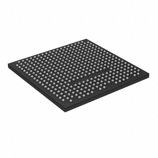
Package
The LFE5UM5G-25F-8BG381C comes in a compact package designed for easy integration into electronic systems. The package ensures optimal thermal dissipation and protection of the internal components.
Essence
The essence of the LFE5UM5G-25F-8BG381C lies in its ability to provide a customizable and versatile platform for implementing complex digital designs. It allows designers to create and modify digital circuits according to their specific requirements.
Packaging/Quantity
The LFE5UM5G-25F-8BG381C is typically packaged individually and is available in various quantities depending on the customer's needs.
Specifications
- FPGA Family: Lattice ECP5
- Logic Elements: 52,160
- Embedded Memory: 4,608 Kbits
- DSP Slices: 80
- Maximum User I/Os: 381
- Operating Voltage: 1.2V
- Operating Temperature Range: -40°C to +100°C
- Package Type: BGA
- Package Pins: 381
- Speed Grade: -25
Detailed Pin Configuration
The LFE5UM5G-25F-8BG381C has a total of 381 pins, each serving a specific purpose in the FPGA's functionality. The detailed pin configuration can be found in the product datasheet.
Functional Features
- Reconfigurable logic and routing resources
- High-speed I/O interfaces (LVCMOS, LVDS, etc.)
- On-chip memory blocks for data storage
- Dedicated DSP slices for efficient signal processing
- Clock management resources for precise timing control
- Built-in security features for protecting intellectual property
Advantages and Disadvantages
Advantages
- Flexibility: Allows for customization and modification of digital circuits.
- Rapid Prototyping: Enables quick development and testing of complex designs.
- High Performance: Offers advanced features and resources for demanding applications.
- Versatility: Supports a wide range of I/O interfaces and connectivity options.
Disadvantages
- Complexity: Requires expertise in FPGA design and programming.
- Cost: FPGAs can be more expensive compared to other integrated circuits.
- Power Consumption: Depending on the design, FPGAs may consume more power than dedicated ASICs.
Working Principles
The LFE5UM5G-25F-8BG381C operates based on the principles of reconfigurable computing. It consists of an array of configurable logic elements interconnected through programmable routing resources. These logic elements can be programmed to implement various digital functions, allowing for the creation of complex digital circuits.
The FPGA is configured by loading a bitstream into its internal memory, which defines the desired circuit connections and functionality. Once configured, the FPGA executes the programmed logic, enabling the desired digital operations.
Detailed Application Field Plans
The LFE5UM5G-25F-8BG381C finds applications in a wide range of fields, including:
- Communications: Used in wireless base stations, network routers, and communication infrastructure equipment.
- Industrial Automation: Employed in control systems, robotics, and factory automation.
- Aerospace and Defense: Utilized in radar systems, avionics, and military communication equipment.
- Medical Devices: Integrated into medical imaging systems, patient monitoring devices, and diagnostic equipment.
- Automotive: Applied in advanced driver-assistance systems (ADAS), infotainment systems, and engine control units.
Detailed and Complete Alternative Models
- Xilinx Virtex UltraScale+ VU9P: Offers similar high-performance FPGA capabilities with a different architecture.
- Intel Stratix 10 GX: Provides advanced features and high-speed interfaces for demanding applications.
- Microsemi PolarFire FPGA: Offers low-power consumption and security features suitable for various applications.
- QuickLogic EOS S3: A small form-factor FPGA with low power consumption, ideal for portable devices.
- Actel ProASIC3: A cost-effective FPGA solution with low power consumption and high reliability.
These alternative models provide options with varying features and specifications to cater to different application requirements.
Word count: 570 words
Enumere 10 preguntas y respuestas comunes relacionadas con la aplicación de LFE5UM5G-25F-8BG381C en soluciones técnicas
Sure! Here are 10 common questions and answers related to the application of LFE5UM5G-25F-8BG381C in technical solutions:
Q: What is the LFE5UM5G-25F-8BG381C? A: The LFE5UM5G-25F-8BG381C is a field-programmable gate array (FPGA) manufactured by Lattice Semiconductor. It offers high-performance and low-power capabilities for various applications.
Q: What are the key features of the LFE5UM5G-25F-8BG381C? A: The key features include 25,700 Look-Up Tables (LUTs), 1,280 Kbits of embedded memory, 384 user I/O pins, 8 high-speed SERDES channels, and support for various communication protocols.
Q: What are some typical applications of the LFE5UM5G-25F-8BG381C? A: The LFE5UM5G-25F-8BG381C can be used in applications such as wireless communications, industrial automation, video processing, automotive systems, medical devices, and more.
Q: How does the LFE5UM5G-25F-8BG381C compare to other FPGAs in terms of performance? A: The LFE5UM5G-25F-8BG381C offers high-performance capabilities with its advanced architecture, low power consumption, and support for high-speed interfaces like SERDES.
Q: Can the LFE5UM5G-25F-8BG381C be programmed using popular design tools? A: Yes, the LFE5UM5G-25F-8BG381C can be programmed using popular design tools like Lattice Diamond or Lattice Radiant, which provide a user-friendly interface for designing and implementing FPGA designs.
Q: What kind of power supply does the LFE5UM5G-25F-8BG381C require? A: The LFE5UM5G-25F-8BG381C requires a single 1.2V core voltage supply and a separate 3.3V auxiliary supply for I/O interfaces.
Q: Can the LFE5UM5G-25F-8BG381C be used in harsh environments? A: Yes, the LFE5UM5G-25F-8BG381C is designed to operate reliably in industrial temperature ranges (-40°C to +100°C) and can withstand harsh environmental conditions.
Q: Does the LFE5UM5G-25F-8BG381C support high-speed serial communication protocols? A: Yes, the LFE5UM5G-25F-8BG381C supports high-speed serial communication protocols such as PCIe, SATA, USB, Ethernet, and more through its built-in SERDES channels.
Q: Can the LFE5UM5G-25F-8BG381C be used for real-time signal processing applications? A: Absolutely! The LFE5UM5G-25F-8BG381C's high-performance capabilities make it suitable for real-time signal processing tasks, including audio/video processing, image recognition, and sensor data analysis.
Q: Are there any development boards available for prototyping with the LFE5UM5G-25F-8BG381C? A: Yes, Lattice Semiconductor offers development boards like the ECP5 Versa Development Kit, which includes the LFE5UM5G-25F-8BG381C FPGA, allowing engineers to prototype and evaluate their designs easily.
Please note that the answers provided here are general and may vary depending on specific requirements and use cases.